0hmX/mt41k512m8da-107-it-p-fanout
This code defines the physical footprint, routing, and layout configuration for a DDR3 memory module using surface-mount pads, vias, and copper traces on a printed circuit board (PCB).
- Version
- 0.2.3
- License
- unset
- Stars
- 0
README.md
# MT41K512M8DA-107 IT:P reusable fanout
Four saved fanout profiles for **one 512 MB ×8 DDR3L RAM**. Place two instances for the AM3352's 1 GB configuration. Uses the original **JLC C2888412 copper pads**, a corrected Micron ×8 signal map, and native `<fanout pcbTracePaths={...}>` geometry. No fanout solver runs when these paths are instantiated.
This follows the organization of [astra/f1c100s](https://tscircuit.com/astra/f1c100s): exported profiles, saved route files, per-profile metrics, and one selectable board preview per profile. These are **BGA escapes with routed edge terminals**, not complete processor-to-memory bus routing or a complete powered RAM module.
## Install and use
```sh
tsci add 0hmX/mt41k512m8da-107-it-p-fanout
```
```tsx
import { MT41K512M8Fanout, LAYOUT_PROFILES } from
"@tsci/0hmX.mt41k512m8da-107-it-p-fanout"
export default () => (
<board width={36} height={22} layers={4}
minTraceWidth={0.12} minViaPadDiameter={0.45} minViaHoleDiameter={0.2}>
<MT41K512M8Fanout name="RAM0" pcbX={-7} layoutProfile="outward_north" />
<MT41K512M8Fanout name="RAM1" pcbX={7} layoutProfile="inward_south" />
</board>
)
```
Use **tscircuit 0.0.2495**, resolving **core 0.0.1884** and **props 0.0.649**, as pinned in this package. Earlier core versions may accept the prop without emitting the saved copper.
## Choose a profile
Directions are local to the unrotated package. A1 is upper left; +Y is north. “Outward” moves left-bank vias left and right-bank vias right; “inward” reverses those X offsets. All offsets are 0.4 mm in X and Y. Rotation changes the whole component and its routes, not its pinout or physical layer names.
| `layoutProfile` | Via X direction | Via Y direction |
|---|---|---|
| `outward_north` (default) | Away from center | +Y |
| `outward_south` | Away from center | −Y |
| `inward_north` | Toward center | +Y |
| `inward_south` | Toward center | −Y |
| Outward north | Outward south |
|---|---|
|  |  |
| Inward north | Inward south |
|---|---|
|  |  |
Preview colors: red is top copper; orange/yellow are inner layers; blue is bottom; magenta marks vias. Separate layer views are available in `previews/*-layers.png`; enlarged top views are in `previews/*-top.png`. Preview board borders are inspection fixtures, not required module outlines. Reserve the **10 × 12.5 mm breakout boundary** plus space for nearby decoupling and routing. Silk/courtyard were moved outside the via field; the 78 JLC copper pads retain their imported coordinates and 0.3839972 mm diameter.
## Connect to parent circuitry
```tsx
<MT41K512M8Fanout
name="RAM0"
layoutProfile="outward_north"
pcbX={-7}
pcbRotation={0}
connections={{
DQ0: ".CPU > .DDR_D0",
DQS_P: ".CPU > .DDR_DQS0",
DQS_N: ".CPU > .DDR_DQSn0",
}}
/>
```
Parent selectors above are illustrative and must match your CPU package. Or use an explicit trace:
```tsx
<trace from=".RAM0 .U1 > .SIG_DQ0" to=".CPU > .DDR_D0" />
```
Outer-column electrical terminals follow pad → top trace → local breakout edge. Inner-column terminals follow pad → top dogbone → through-via → onward trace → local breakout edge at **X = ±5.0 mm**. Exit Y matches the source ball except DQS and CK, whose adjacent terminals are centered around the pair midpoint with 0.32 mm center spacing. Columns 1/9 stay on top without vias, 2/8 on inner2, and 3/7 on inner1. Parent routing begins at that edge terminal on its declared layer. The local boundary is **10 × 12.5 mm**: the 8 × 10.5 mm package body plus exactly **1 mm padding on every side**, independent of the host-board edge. `PACKAGE_BODY`, `FANOUT_PADDING_MM` and `BREAKOUT` expose these dimensions.
Inner-layer via exits use direct diagonal approaches, with no copper-layer bend sharper than 45°. DQS and CK retain their wider row spacing through the via field and converge only beyond X = ±3.8 mm; the convergence segments have at least 0.5 mm copper clearance from every via.
Every saved path has a real electrical `<trace>` to an instance-specific local net. This module contains **no power or ground copper pours**. Therefore VDD/VDDQ and VSS/VSSQ also reach edge terminals. A power/ground edge route may be omitted only in a design that provides and verifies an actual connection to its assigned continuous copper region. Inner1 and inner2 contain lateral breakout routes. Bottom has no saved lateral traces, but still contains through-via barrels; this module does not create a plane there.
Exports:
- `MT41K512M8Fanout` (also default), with `name`, `layoutProfile`, `pcbX`, `pcbY`, `pcbRotation`, `schX`, `schY`, and `connections`.
- `LAYOUT_PROFILES`, `PROFILE_LAYOUTS`, `LayoutProfile`, `RULES`, `BREAKOUT`, `getExitLayer`.
- `getRamFanoutTracePaths(profile)`: a fresh, schema-validated copy on each call.
- `PIN_MAP`, `EXTERNAL_TERMINALS`. The `./profiles` package entrypoint also exports profile metadata.
Signal terminals include `A0`–`A15`, `BA0`–`BA2`, `DQ0`–`DQ7`, `DM`, `DQS_P/N`, `CK_P/N`, `CS_N`, `RAS_N`, `CAS_N`, `WE_N`, `CKE`, `ODT`, `RESET_N`, `ZQ`, `VREFCA`, and `VREFDQ`. Supply terminals are **per ball**, for example `VDD_A2`, `VDDQ_C1`, `VSS_A1`, `VSSQ_D1`. Connect **every** VDD/VDDQ supply ball and VSS/VSSQ ground ball on the parent board; no supply grouping is hidden inside this fanout.
`ball_A1` means the physical A1 location (ground). `SIG_A1` means the address signal located on **L7**. This naming prevents the collision found in the original import.
## Geometry and performance intent
Every profile has:
- **78 pads, 72 saved copper routes, 50 through-vias**.
- **0.12 mm traces** on top and the assigned exit layer; **0.45 mm through-via copper / 0.20 mm drill**.
- All **72 routed terminals reach the left or right breakout edge**, including power and ground.
- At least **0.10 mm clearance** between foreign copper on every layer, checked from emitted geometry (see generated metrics for measured values).
- **Pre-tuned physical lengths** for DQ0–7/DM/DQS and separately A0–15/BA0–2/control/CK, verified to **≤0.005 mm group skew**.
- DQS and CK each have a **>0.9 mm parallel tail on inner1**, 0.20 mm copper gap, and adjacent edge terminals. Their uncoupled BGA escape sections remain included in full-route length checks.
- Short corrections use one broad 45-degree offset; larger corrections use up to two spaced tuning sections. Sub-trace-width tuning segments are rejected. Matching is performed during generation and stored in each cache; no matching solver runs on import.
NC balls **A3, F1, H1, F9, H9** have no fanout. **A7 (TDQS#)** also has no fanout: this package assumes TDQS is disabled and B7 is used as DM. It does not program the DRAM mode registers.
Include the full edge-route lengths and their skew in the carrier's timing budget; these routes do **not** prove equal electrical delay or 800 MT/s operation. The pairs have verified physical geometry, but impedance and electrical delay remain unverified: via parasitics, actual dielectric stackup, complete pair coupling and return paths need board-level analysis. No speed/IBIS validation was performed.
For AM3352, account for these paths in the complete byte-lane and clock/address routing. TI specifies matching within each byte, not between bytes. Provide the required two-device CK/address topology and termination, uninterrupted reference planes, supply/ground connections, decoupling, VREF filtering and ZQ resistor on the parent board. Those components are outside this fanout package.
## Provisional stackup and matching assumptions
`src/timing.ts` records the user-approved generic assumptions with their basis: 1.6 mm FR-4, nominal Er 4.2, 35 µm copper, illustrative copper-layer depths 0/0.2/1.4/1.6 mm, and nominal 50 Ω single-ended / 100 Ω differential targets. These are **placeholders**, not fabrication measurements or achieved impedance. The existing 0.12 mm trace width is retained; pair gap is widened to 0.20 mm for more separation; they were not obtained from an impedance solver.
The four-layer profiles pass physical routing and length checks, so no six/eight-layer variants were added. Both paired tails use inner1. Outer-column signals stay on top; other inner-column signals use inner2; equal planar lengths across those layers do **not** imply equal propagation delay. Once the actual stackup is supplied, recalculate trace width/gap and dielectric/via delay, then regenerate and revalidate. Power, ground, VREF and ZQ are not timing-matched bus members. Their routes still reach the boundary because this module has no pours or local support components.
The 0.005 mm limit is a geometric acceptance threshold, not a fabrication-accuracy claim. Full-interface DDR3 limits and topology remain host-board responsibilities. Constraints and assumptions are exported as `PAIRS`, `MATCH_GROUPS`, `TUNING` and `PROVISIONAL_STACKUP`.
## Verification
[Detailed design audit](https://registry-api.tscircuit.com/package_files/download?package_name_with_version=0hmX%2Fmt41k512m8da-107-it-p-fanout%400.2.1&file_path=docs%2Fdesign-audit.md) includes sources and limits. Four per-profile metrics files and compiled Circuit JSON files are under `src/generated/`; saved paths are in `*.trace-paths.json`.
```sh
bun install
bun run generate
bun run build
bun run verify
bun test
bun run typecheck
```
Completed checks cover emitted copper, all 78 physical pads, ×8 signal identities, route starts, exits, layers, via sizes, geometric clearances, and a two-instance translated/rotated placement with host traces continuing from saved inner1 and top exits. Netlist and placement checks pass; no copper shorts were detected. Preview warnings about missing electrical pin attributes are expected for this fanout-only model and do not qualify it as a complete functional RAM circuit.
Related Packages
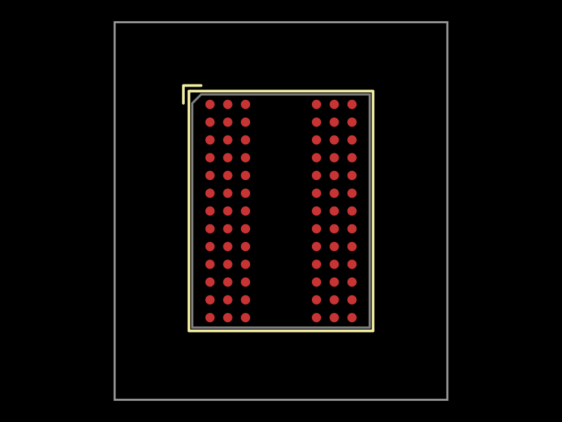 More from this author0hmX/mt41k512m8da-107-it-p-footprintsThis code defines the mechanical and physical layout of a Micron digital ball grid array (FBGA) package with 78 balls, including pin positions, footprint geometry, PCB pads, and silkscreen outlines for surface-mount integration.
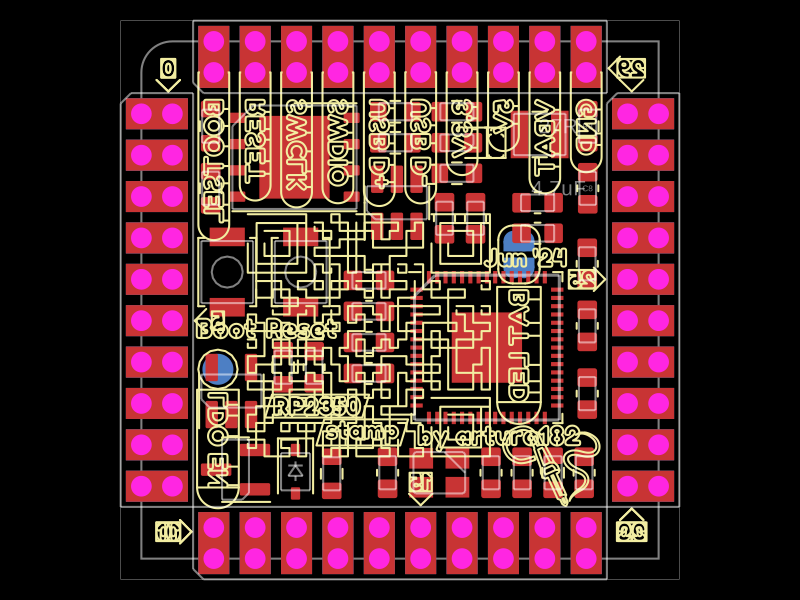 Similar packagetechmannih/imported-rp2350-stamp-boardThis code defines a detailed PCB layout with multiple layers, including the physical outline, component footprints, drilling holes, SMT pads, silkscreen markings, and courtyard outlines for component placement and board edges.
 Discover something newShiboSoftwareDev/mspm0g3507-usb-c-dev-boardThe circuit assembles a USB-C port with integrated ESD protection, power regulation, UART interface, and microcontroller (MSPM0G3507) with supporting components for USB data lines, CC termination, I2C, SPI, reset circuitry, and indicator LEDs.