0hmX/mt41k512m8da-107-it-p-fanout
This code defines the physical footprint, routing, and layout configuration for a DDR3 memory module using surface-mount pads, vias, and copper traces on a printed circuit board (PCB).
- Version
- 0.2.3
- License
- unset
- Stars
- 0
docs/design-audit.md
# Design audit — 2026-09-10

## Manufacturer evidence

- [Micron 4Gb DDR3L datasheet, Rev. R 09/18, hosted by LCSC](https://atta.szlcsc.com/upload/public/pdf/source/20241017/DD693FFA66FA4C721D9CFF3534518DFE.pdf): Figure 6, page 17 is the top-view x4/x8 ball map; Figure 10, page 25 is the 78-ball DA package. The **x8** meaning of multiplexed entries was used: D2=DQ6, E3=DQ4, E7=DQ7, E8=DQ5, B7=DM (TDQS disabled). Physical L7 is address A1; physical A1 is VSS. Package dimensions are 8 × 10.5 mm and 0.8 mm pitch, with columns 4–6 absent. The map was transcribed from the actual figure, not copied from the incomplete JLC signal labels.
- [JLCPCB C2888412](https://jlcpcb.com/partdetail/MicronTech-MT41K512M8DA_107_ITP/C2888412): original pad coordinates and 0.3839972 mm pad diameter retained. Non-copper silk and courtyard are adjusted for the added via field. The previous footprint audit is [published separately](https://tscircuit.com/0hmX/mt41k512m8da-107-it-p-footprints).
- [TI AM335x datasheet SPRS717L](https://www.ti.com/lit/ds/symlink/am3352.pdf), sections 7.7.2.3.3–7.7.2.3.6, Tables 7-68 and 7-69: minimize vias, control clock/address skew, and match DQ/DM to its own byte strobe. Table 7-69 gives 25 mil (0.635 mm) DQ and DQS-to-DQ skew and 5 mil (0.127 mm) DQS-pair skew for the **complete interconnect**. No cross-byte length matching is recommended. Our escapes consume equal planar length; these limits are not certifications of this standalone module. TI also discusses return-current transitions, VREF bypassing and termination.
- [JLC manufacturing capabilities](https://jlcpcb.com/capabilities/Capabilities%2C/): 0.20 mm drill with 0.45 mm via diameter is a published conventional option. The parent board's thickness, stackup, solder-mask, paste, annular rings and fabrication quote still control manufacturability.

## Revised edge-routing contract

All four profiles now extend all 72 electrical connections to X = ±5.0 mm on an 10 × 12.5 mm local breakout boundary. The five NC balls and disabled TDQS# retain their documented omissions. Every path starts at the original pad. Outer columns 1/9 run directly on top to the edge with no via. Inner columns use their profile's ±0.4 mm dogbone, pass through a conventional through-via, then return to the ball's Y coordinate and continue to the edge. Timing-group members receive one or two broad tuning sections outside the via field. Differential pairs converge symmetrically to adjacent terminals and retain a straight parallel tail longer than 0.9 mm. Columns 1/9 use top, 2/8 inner2, and 3/7 inner1. The core emits full-depth via barrels for these layer transitions, verified on all four layers.

No power or ground pours exist in this package. Power and ground therefore also have explicit edge routes. A future pour-based variant may omit their edge extensions only after verifying actual same-net copper contact and continuity to the supply interface. The current inner layers carry routes and cannot be treated as uninterrupted reference planes.

All DQ/DM/DQS routes are now physically matched as one byte group; address/bank/control/CK routes form a second matched group. Both groups and each differential pair must have no more than 0.005 mm planar skew in compiled geometry. Pair tails share inner1 with 0.12 mm width and 0.20 mm copper gap. The complete dogbone, post-via run and tuning cells count toward the reported lengths.

`src/timing.ts` documents user-approved generic FR-4 assumptions: 1.6 mm board, Er 4.2, 35 µm copper, illustrative 0/0.2/1.4/1.6 mm copper-center depths and 50/100 Ω nominal impedance targets. They are placeholders, not a manufacturer stackup. Trace width/gap currently follow geometric clearance; no impedance solver or layer/via delay compensation has been applied. Four layers suffice for geometric matching. Six/eight-layer routing can be reconsidered with the real stackup. Different signal layers mean planar matching is not electrical-delay signoff.

## Verification

The geometry verifier checks compiled Circuit JSON: all 78 pads, 72 routes and exits, all 50 full-depth vias, source identities, continuous wire/via layer transitions, exact edge endpoints and matching breakout-point layers, pair tail layer/spacing/length, byte and address/control/clock group skew, and minimum 0.10 mm foreign-copper clearance across all four layers. NC pads participate as copper obstacles too. CLI checks cover netlists, schematic/PCB placement, builds and shorts. A host fixture places two modules, rotates the second by 90°, and routes DQ0 from the first module's inner1 edge and ODT from its top edge to external through-hole headers. API tests check independent cache copies, invalid inputs and x8 pin identities.

Generated metrics, compiled Circuit JSON and previews are regenerated with the saved paths. No electrical simulation, impedance extraction, return-path analysis or assembled-board testing is included. Host continuation is demonstrated for DQ0; arbitrary congested host routing is not guaranteed.

## Tuning geometry revision

The initial five-cell matcher spread small corrections across repeated bends shorter than the trace width. It passed centerline length checks but was an unsuitable geometry choice. The revised generator uses a single 45-degree trapezoid for small corrections and up to two broad chamfered trombones for larger corrections. Inner-layer tuning cells occupy 0.65 mm horizontally at 0.8 mm pitch. Top-layer ODT/CKE use two 0.6 mm cells at 0.72 mm pitch and the vertical room beside their adjacent NC rows. No nonzero tuning segment may be shorter than the 0.12 mm trace width. Paired tails remain straight, and matching/clearance thresholds are unchanged.

This improves the actual copper geometry rather than just rendering. It remains a local fanout with no reference pours, decoupling or processor routing. Its appearance and planar matching must not be presented as evidence of a production-ready DDR interface.

## Outer-column top routing

All 22 populated electrical pins in columns 1/9 remain entirely on top, eliminating 22 unnecessary through-vias per module. The remaining 50 inner-column routes retain their original dogbone placements and full-depth barrels. Matching accounts for the changed top-only planar lengths. The validator asserts that every outer route contains only top-layer wire segments and no via, and checks all 72 edge exits. Host tests cover continuation from both top and inner1. Bottom has no saved lateral tracks; it is not automatically a ground plane.

## 1 mm padding contract

The local fanout boundary is derived from the 8 × 10.5 mm package body plus 1 mm on each side: 10 × 12.5 mm, with X exits at ±5 mm. Padding is measured from the component body, not the pad centers, courtyard or preview-board boundary. Tuning was regenerated inside that boundary while retaining the existing 0.005 mm matching tolerance and 0.10 mm copper-clearance rule. Pair tails are about 0.96 mm after moving convergence outside the via field; their gap and matching are unchanged. Route bounds are checked explicitly. The existing footprint labels and silkscreen are annotations and are not the fanout boundary.

## Inner-layer corner and pair-spacing revision

All inner-column via exits now run directly on a 45-degree diagonal into their row channel, replacing the vertical/horizontal L. The via positions, layer count and 1 mm boundary remain fixed; both north/south and inward/outward variants are regenerated. The DQS and CK pair tails now have a 0.20 mm edge gap (0.32 mm center spacing), wider than the prior 0.12 mm gap. This is still a provisional geometric choice, not an impedance result.

The validator rejects every copper-layer bend greater than 45 degrees and retains full-route matching, minimum feature size, all-layer clearance and host-continuation checks. Dense via channels still set the minimum foreign-copper clearance; widening the pairs does not imply that every unrelated via/trace gap became wider. Copper on other layers in a combined screenshot is not a same-layer short.

## Pair convergence outside the via field

DQS and CK preserve the BGA row spacing until X = ±3.8 mm before converging symmetrically to their 0.20 mm copper gap. The complete convergence segment must clear every via annulus by at least 0.5 mm, including trace half-width. This replaces the crowded early convergence near the outer via column. The paired straight tail is approximately 0.96 mm and continues at the host boundary. Full planar lengths are unchanged by translating the convergence outward. Matching, 45-degree turns, top outer routes and the 1 mm boundary remain enforced.

The all-layer bend audit also passes for the two-instance host-routing fixture. The prohibition applies to copper traces, not component outlines or drawing annotations.
Related Packages
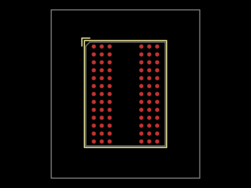 More from this author0hmX/mt41k512m8da-107-it-p-footprintsThis code defines the mechanical and physical layout of a Micron digital ball grid array (FBGA) package with 78 balls, including pin positions, footprint geometry, PCB pads, and silkscreen outlines for surface-mount integration.
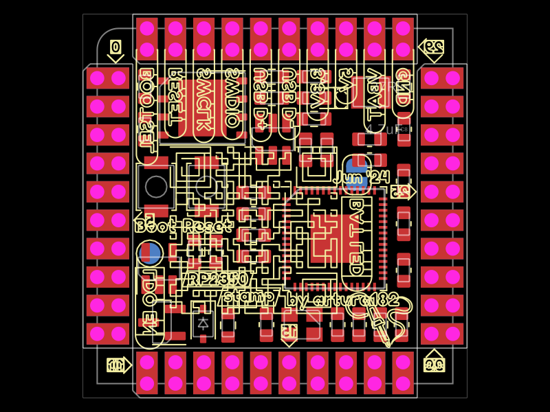 Similar packagetechmannih/imported-rp2350-stamp-boardThis code defines a detailed PCB layout with multiple layers, including the physical outline, component footprints, drilling holes, SMT pads, silkscreen markings, and courtyard outlines for component placement and board edges.
 Discover something newShiboSoftwareDev/mspm0g3507-usb-c-dev-boardThe circuit assembles a USB-C port with integrated ESD protection, power regulation, UART interface, and microcontroller (MSPM0G3507) with supporting components for USB data lines, CC termination, I2C, SPI, reset circuitry, and indicator LEDs.