0hmX/mt41k512m8da-107-it-p-fanout
This code defines the physical footprint, routing, and layout configuration for a DDR3 memory module using surface-mount pads, vias, and copper traces on a printed circuit board (PCB).
- Version
- 0.2.3
- License
- unset
- Stars
- 0
src/timing.ts
import { PIN_MAP } from './pin-map'
// Preliminary geometry limits, deliberately tighter than the complete-interface
// DDR3 limits in TI AM335x SPRS717L Tables 7-68/69 (5 mil pair, 25 mil byte skew).
// They constrain planar copper length only, not propagation delay or impedance.
export const PAIRS: readonly (readonly string[])[] = [['DQS_P','DQS_N'],['CK_P','CK_N']]
export const MATCH_GROUPS = {
 byte: ['DQ0','DQ1','DQ2','DQ3','DQ4','DQ5','DQ6','DQ7','DM','DQS_P','DQS_N'],
 addressControlClock: [...Array.from({length:16},(_,i)=>`A${i}`),'BA0','BA1','BA2','CS_N','RAS_N','CAS_N','WE_N','CKE','ODT','RESET_N','CK_P','CK_N'],
} as const
// Bring pairs together beyond the entire through-via field, keeping their
// full BGA row separation until X=±3.8 mm. This leaves ~0.96 mm of paired tail
// inside the 1 mm body padding; host routing continues the pair at the edge.
export const TUNING={maxSkewMm:.005,pairGapMm:.20,pairCenterSpacingMm:.32,startX:3.2,topTuningStartX:3.4,pairConvergenceStartX:3.8,minPairedTailMm:.9} as const
// USER-APPROVED PLACEHOLDERS, not manufacturer data or a field-solver result.
// 1.6 mm / 35 um copper and Er=4.2 are generic FR-4 example values.
// Copper center depths are a symmetric illustrative four-layer stack; actual
// laminate/prepreg thickness and frequency-dependent Er must replace these.
// 50 ohm / 100 ohm are nominal DDR design targets (TI SPRS717L Table 7-62 and
// Table 7-69 note 11), not impedances achieved by the present .12/.12 geometry.
// Pair gap .20 mm provides more separation than the original .12 mm gap;
// width .12 mm is the existing BGA escape width. Recalculate width/gap and
// layer/via delay, then regenerate and revalidate when the real stack arrives.
export const PROVISIONAL_STACKUP={
 status:'placeholder-not-impedance-verified',boardThicknessMm:1.6,copperThicknessMm:.035,
 dielectricEr:4.2,copperCenterDepthMm:{top:0,inner1:.2,inner2:1.4,bottom:1.6},
 targetSingleEndedOhms:50,targetDifferentialOhms:100,
} as const
export function getEdgeY(pin:typeof PIN_MAP[number]) {
 const pair=PAIRS.find(pair=>pair.includes(pin.terminal))
 if(!pair)return pin.y
 const mate=PIN_MAP.find(p=>p.terminal===pair.find(n=>n!==pin.terminal))!
 return (pin.y+mate.y)/2+Math.sign(pin.y-mate.y)*TUNING.pairCenterSpacingMm/2
}
Related Packages
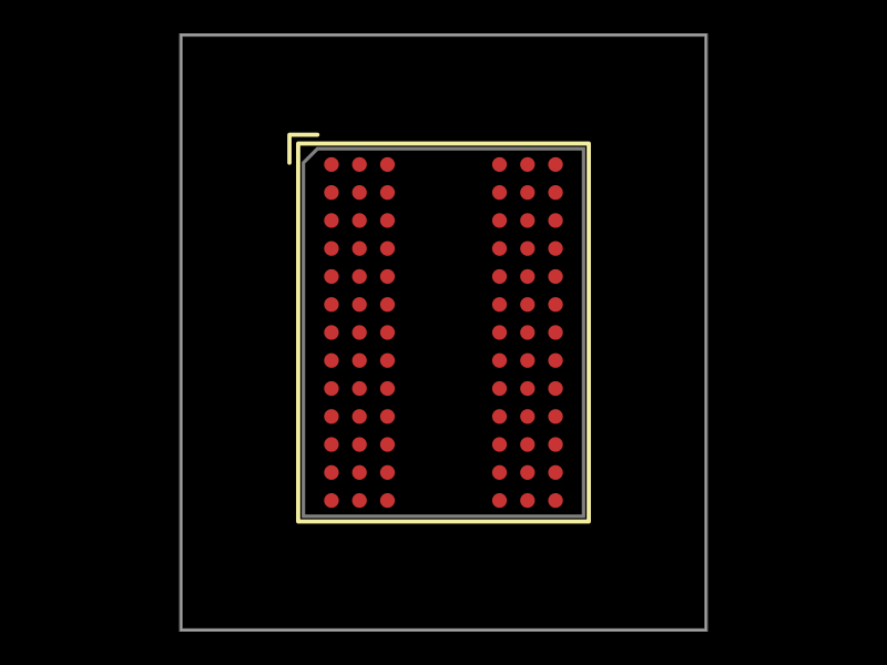 More from this author0hmX/mt41k512m8da-107-it-p-footprintsThis code defines the mechanical and physical layout of a Micron digital ball grid array (FBGA) package with 78 balls, including pin positions, footprint geometry, PCB pads, and silkscreen outlines for surface-mount integration.
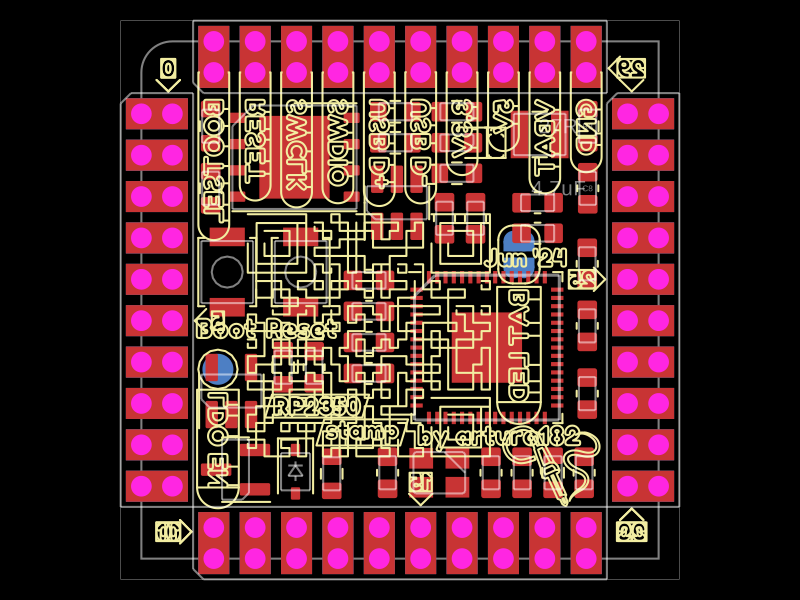 Similar packagetechmannih/imported-rp2350-stamp-boardThis code defines a detailed PCB layout with multiple layers, including the physical outline, component footprints, drilling holes, SMT pads, silkscreen markings, and courtyard outlines for component placement and board edges.
 Discover something newShiboSoftwareDev/mspm0g3507-usb-c-dev-boardThe circuit assembles a USB-C port with integrated ESD protection, power regulation, UART interface, and microcontroller (MSPM0G3507) with supporting components for USB data lines, CC termination, I2C, SPI, reset circuitry, and indicator LEDs.