0hmX/mt41k512m8da-107-it-p-footprints
This code defines the mechanical and physical layout of a Micron digital ball grid array (FBGA) package with 78 balls, including pin positions, footprint geometry, PCB pads, and silkscreen outlines for surface-mount integration.
- Version
- 0.1.1
- License
- unset
- Stars
- 1
README.md
# MT41K512M8DA-107 IT:P footprints
Footprint-only tscircuit package for **MT41K512M8DA-107 IT:P**, package code **DA**, 78 balls, **8 × 10.5 mm**, **0.8 mm pitch**. Created and checked 2026-09-10.
**Result:** the original JLC/EasyEDA import has the correct ball-center geometry. Its maximum coordinate difference from the nominal grid is only **0.000108 mm (0.108 µm)**, attributable to rounding. A custom footprint is useful for clean physical ball names, exact metric coordinates, the DA body drawing, and explicit pad-size selection. It is not needed to repair a gross placement error.
## Reference versus ours
| Micron manufacturer drawing — original page 25 | Our footprint — from compiled tscircuit geometry |
|---|---|
| 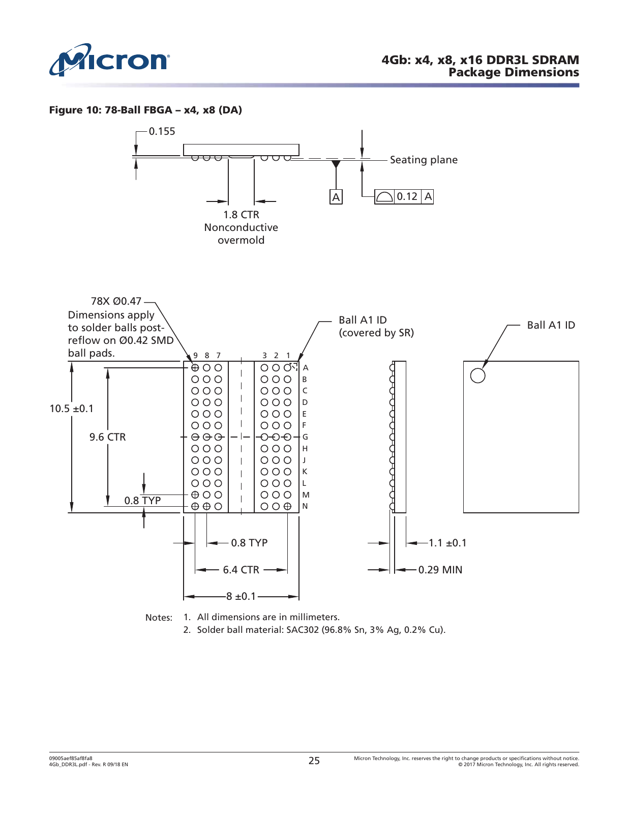 | 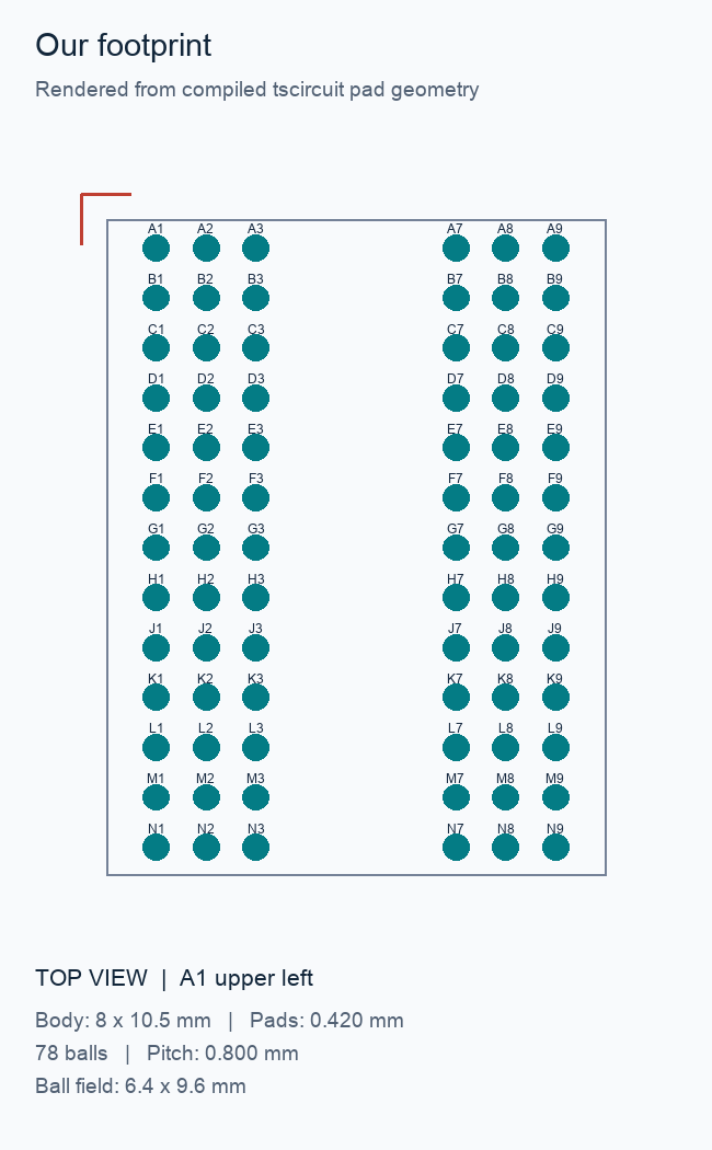 |
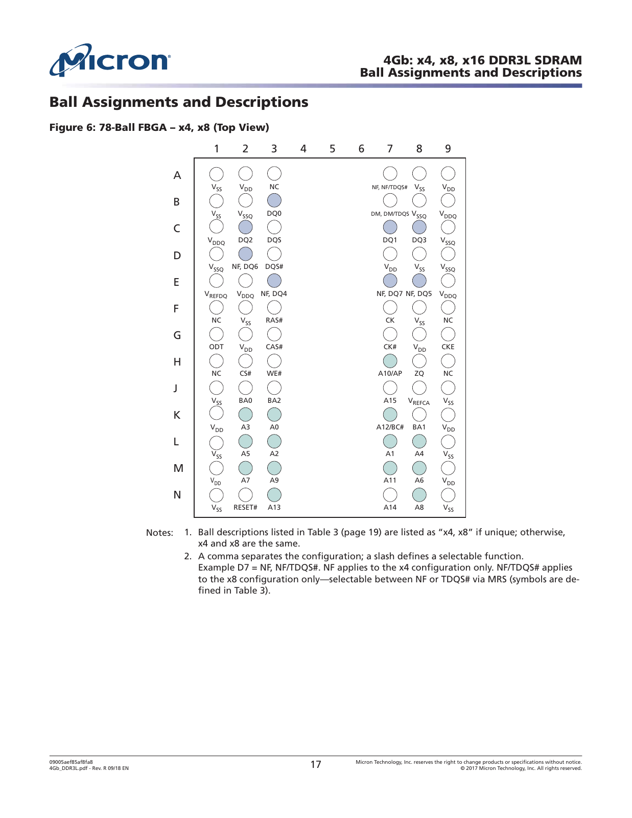
**View direction matters:** the ball-side mechanical view on Micron page 25 has A1 on the right. Our PCB drawing is viewed from the component side, with A1 upper left, as in Micron's explicitly labeled top view on page 17 below. Do not mirror the PCB footprint to resemble the bottom view.
| Micron top-view ball map — original page 17 | KiCad pad overlay on our compiled footprint |
|---|---|
|  | 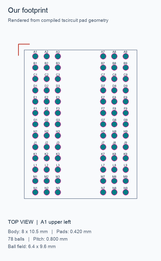 |
In the overlay, teal is our compiled copper and magenta is the independently parsed KiCad pad perimeter. All 78 centers and diameters coincide after converting KiCad's Y-down coordinates to tscircuit's Y-up coordinates. The KiCad body is different and is not used for our body outline.
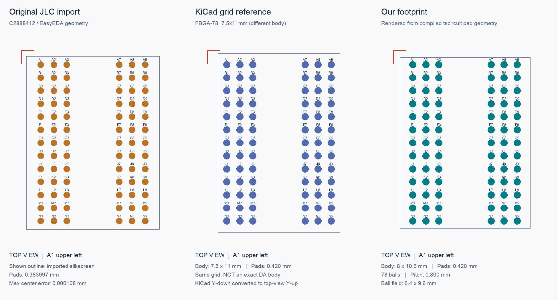
The comparison images are engineering renders of the saved source data, not screenshots from the KiCad application. The Micron images are unaltered full-page PDF renders. An actual tscircuit board SVG is available in [images/tscircuit-pcb.svg](https://registry-api.tscircuit.com/package_files/download?package_file_id=6536071a-a439-415c-a108-ec66f35a76e0).
## Measured comparison
| Property | Micron DA drawing | Original import | KiCad grid reference | Our footprint |
|---|---|---|---|---|
| Balls | 78 | 78 | 78 | 78 |
| Rows | A–H, J–N | Same physical rows | Same | Same |
| Populated columns | 1, 2, 3, 7, 8, 9 | Same | Same | Same |
| Pitch | 0.8 mm | Approx. 0.8 mm | 0.8 mm | 0.8 mm |
| Center span X × Y | 6.4 × 9.6 mm | 6.399784 × 9.600184 mm | 6.4 × 9.6 mm | 6.4 × 9.6 mm |
| Body | 8 ±0.1 × 10.5 ±0.1 mm | No complete body fab rectangle; silk ~8.152 × 10.652 mm | 7.5 × 11 mm, different package | 8 × 10.5 mm fab outline |
| PCB copper pad diameter | Not an explicit PCB land-pattern specification | 0.3839972 mm | 0.42 mm | **0.42 mm** |
| Minimum adjacent copper gap | — | ~0.416 mm | 0.38 mm | 0.38 mm |
| A1 physical ball label | A1 | Renamed `A11` in chip wrapper | A1 | `A1`, `ball_A1`, `pin1` |
### Pad-size decision
The default **0.42 mm circular copper land** matches the independently available KiCad grid reference. It is a documented layout choice, **not a claim that Micron explicitly mandates a 0.42 mm PCB copper land**. The original import's 0.384 mm pads are smaller; this comparison does not prove they are unmanufacturable.
Micron's drawing calls out 0.47 mm post-reflow solder balls and refers to 0.42 mm SMD ball pads in its package-dimension note. Those values must not be blindly equated with a complete PCB land, mask, and stencil specification. This package defines copper geometry with uncovered top-side pads; explicit solder-mask expansion and paste reduction remain board/fabrication-process settings. No JLC assembly qualification or manufactured-board test was performed.
The courtyard is 9.1 × 11.6 mm, centered, and includes the external A1 silk marker. The fabrication outline is the nominal body with a small A1 chamfer; the silk is an external outline. These outline choices are authored here, not taken from Micron as required assembly clearances.
## Use in tscircuit
```tsx
import { MicronDaFbga78Footprint, ballPinLabels } from "./src/index"
<chip
name="U1"
pinLabels={ballPinLabels}
footprint={<MicronDaFbga78Footprint />}
/>
```
The exported package contains **only physical footprint geometry and physical ball identifiers**. It has no DRAM schematic symbol, no electrical signal mapping, no nets, and no 3D model. `examples/preview.circuit.tsx` is a separate inspection fixture.
Use `ball_A1` when clarity is important: ball **A1** is a physical location, whereas the DRAM address signal **A1** is on physical ball **L7**. The numerical `pin1`…`pin78` aliases preserve the original import's column-major order; the complete mapping is in [src/balls.json](https://registry-api.tscircuit.com/package_files/download?package_file_id=9f4c08ad-1440-4153-98cf-7f69d4620745).
The original chip wrapper loses or renames electrical labels, including DQ4–DQ7 and DM. Do not use it as a verified DRAM symbol. It is preserved under `evidence/` only for the audit. This new footprint intentionally does not attempt to supply an electrical symbol.
## Reproduce the checks
Tested with tscircuit **0.0.2462** and Bun. From this directory:
```sh
bun install
bunx tsci check netlist examples/preview.circuit.tsx
bunx tsci check schematic-placement examples/preview.circuit.tsx
bunx tsci check placement examples/preview.circuit.tsx
bun run build
bun run verify
bunx tsci check shorts dist/examples/preview/circuit.json
```
Completed results:
- Netlist check: 0 errors / 0 warnings; all pins intentionally unconnected.
- Schematic placement: 0 errors / 0 warnings.
- PCB placement: no placement issues, 0 errors / 0 warnings.
- Build: successful. It reports expected electrical-metadata warnings because the fixture intentionally has no power attributes or complete schematic sheet.
- Independent geometry verification: all 78 compiled pads match the transcribed Micron grid and KiCad reference coordinates; all 78 physical identities are unique.
- Copper shorts check: no shorts detected on the preview fixture.
[Machine-readable verification report](https://registry-api.tscircuit.com/package_files/download?package_file_id=9b44088b-9a8e-416d-9edc-ee6e4462c7d2) · [Source checksums](https://registry-api.tscircuit.com/package_files/download?package_file_id=5490cb62-a996-4e13-93ad-6ecc4830167f)
These checks cover physical geometry and pad identity. They do not validate a future RAM symbol, power distribution, DDR timing, signal integrity, or board routing.
## Sources and provenance
1. **Micron, 4Gb: x4, x8, x16 DDR3L SDRAM, Rev. R, September 2018**, Figure 10, page 25 (DA mechanical drawing), and Figure 6, page 17 (top-view ball map). [Manufacturer-authored PDF hosted by LCSC](https://atta.szlcsc.com/upload/public/pdf/source/20241017/DD693FFA66FA4C721D9CFF3534518DFE.pdf). The filename is a distributor identifier; the actual downloaded document title/revision and DA figure were inspected. Source-page render images are included above for audit.
2. **KiCad official footprint library**, [FBGA-78_7.5x11mm_Layout2x3x13_P0.8mm](https://github.com/KiCad/kicad-footprints/blob/7ebfa6b23cc292a56f751b7b5f4a0e12eeef69dd/Package_BGA.pretty/FBGA-78_7.5x11mm_Layout2x3x13_P0.8mm.kicad_mod), pinned commit `7ebfa6b23cc292a56f751b7b5f4a0e12eeef69dd`. It references SK hynix, not this Micron body. Used as an independent grid/land reference only. The inspected tree contained no exact 8 × 10.5 mm FBGA-78 footprint. [KiCad library licensing](https://www.kicad.org/libraries/license/); the copied reference remains under its upstream license.
3. **JLCPCB/EasyEDA C2888412**, [selected industrial RAM listing](https://jlcpcb.com/partdetail/MicronTech-MT41K512M8DA_107_ITP/C2888412). Imported using `tsci import C2888412 --jlcpcb --use-exact-footprint`. Original output is preserved for comparison, not exported as the package API.
4. **Ultra Librarian**, [MT41K512M8DA-107 AAT:P TR](https://app.ultralibrarian.com/details/9d7455ff-7f4d-11eb-9033-0a34d6323d74/Micron/MT41K512M8DA-107-AAT-P-TR) lists an Altium-compatible footprint for the automotive variant. No Altium library file was obtained or geometrically verified; this listing is not counted as an independent dimensional check.
Package source is newly authored. Reference drawings and library files retain their owners' rights. Registry package name: `mt41k512m8da-107-it-p-footprints`.
Related Packages
 More from this author0hmX/tps6521401vafr-pmicThis code models and visualizes the pin configuration and electrical attributes of the TPS6521401 voltage supervisor IC in a specific WQFN-HR package.
 Similar packageAnasSarkiz/vibe_GoblinThese code snippets define various physical electronic components such as ICs, connectors, sensors, LEDs, and chips, specifying their pin layouts, footprint pads, silkscreen markings, courtyard outlines, and 3D CAD models for placement on PCB boards.
 Discover something newShiboSoftwareDev/mspm0g3507-usb-c-dev-boardThe circuit assembles a USB-C port with integrated ESD protection, power regulation, UART interface, and microcontroller (MSPM0G3507) with supporting components for USB data lines, CC termination, I2C, SPI, reset circuitry, and indicator LEDs.