AnasSarkiz/ble-pedometer
This code defines and configures various electronic hardware components such as surface-mount resistors, crystals, diodes, transistors, connectors, and switches with their physical footprints, schematic symbols, and 3D CAD models for PCB assembly.
- Version
- 1.0.7
- License
- unset
- Stars
- 0
README.md
# BLE Pedometer Rev A

A one-sided, 60 × 38 mm, four-layer rechargeable BLE activity tracker. Engineering-review revision; not a released JLCPCB manufacturing package. See [DRC_REPORT.md](DRC_REPORT.md) for measured checks and [FABRICATION_NOTES.md](FABRICATION_NOTES.md) for the remaining export and qualification gates. Never order an older local Gerber archive.

## Implemented hardware

- CC2340R52E0RGER BLE MCU, 48 MHz crystal, DC/DC network, reset and SWD access.
- BMA400 on I²C at 0x14, with separate activity/step and double-tap interrupts.
- **BQ25186DLHR WSON charger** at 0x6A, replacing the blocked BQ25150 ball array. USB power path, battery NTC/button input, charge-enable pull-up and status interrupts.
- **TPS7A0233DBVR** independent, always-on nominal 3.3 V regulator. The raw charger output is not the MCU supply.
- BQ27427YZFR fuel gauge at 0x55 in the cell current path.
- Power-gated 64×32 OLED connector with isolated I²C lines.
- Johanson chip antenna, TI RF filter, DNP tuning capacitors and copper keepouts.
- Power-only USB-C, protected-LiPo/NTC connector and wake button.
- Three ANSI B schematic sheets, eight named sections and 58 component placements.

The charger redesign removes the old IMAX resistor and TS bias resistor. Charge control and battery qualification must follow [CHARGER_BRINGUP.md](CHARGER_BRINGUP.md); old BQ25150 register instructions no longer apply.

## Build and review

```sh
bun install --frozen-lockfile
bun run check:review
bun run export:schematics
bun run check:fabrication
bun run export:manufacturing-review
```

The source-review checks cover TypeScript, regression tests, sheet/placement snapshots, netlist and schematic placement. Full routed DRC, physical via validation and independent shorts are separate gates. The pinned CLI can exit zero while reporting build errors; the fabrication gate reads the actual emitted records.

Use `export:manufacturing-review`, not the pinned CLI's `tsci export -f gerbers`: that CLI still bundles obsolete exporters. The new command renders the unchanged source with the public core API and calls pinned official Gerber 0.0.104, BOM 0.0.17 and PnP 0.0.13 libraries. It checks actual through-board drill files and the exact 50 fitted-part inventory. Package descriptions are supplied by the BOM library's documented resolver from `assembly-parts.ts`, with strict MPN/supplier matching. No generated geometry or CSV rows are patched.

Each run creates a separate `dist/manufacturing-review-*` directory and records its Circuit JSON hash and outstanding sign-offs in `review.json`. Run the shorts and silkscreen commands against that directory's `circuit.json`. **These are review files, not an order release:** all 50 placements currently lack supplier pin-1 calibration, so their original rotations are preserved but require JLCPCB orientation/centroid review. No calibration is guessed. See `PACKAGE_UPDATE_REPORT.md` for measured results.

The via minima remain **0.30 mm drill / 0.45 mm pad** with blind/buried routing disabled. The solder mask is green. A clean geometric DRC does not certify exporter correctness, assembly, RF or battery safety.

Silkscreen references use compact prefixes (`C10` for `C10_VDDR_100N_A`) without renaming schematic, netlist or BOM components. All 58 references have individually assigned positions in `board-silkscreen.tsx`; imported/default reference text is replaced using native PCB styling while footprint outlines and pin-one marks remain. After a full build, run `bun scripts/check-silkscreen.ts` to check conservative text envelopes against labels, pads, drills and courtyards. This does not replace final vendor artwork/CAM review.

## Layout and firmware

The board grew from 42 × 26 mm to 60 × 38 mm. Power/battery components occupy the left side; display switching is near its connector; MCU, motion and RF occupy the right. SWD pads form a 2.2 mm-pitch row. The enlarged outline requires new enclosure and antenna qualification. All placements live in `pcb-layout.ts`; schematic assignments live in `schematic-layout.ts`.

Program through SWDIO, SWDCK, RESET, GND and SYS_VDD-reference test pads with a compatible TI debug probe. Do not attach two competing power supplies. Firmware is not included or bench-tested.

At startup hold charge enable high, display power off and display bus disconnected. Configure and verify the charger before enabling charging; configure the gauge for the qualified cell and BMA400 for interrupt-driven activity/tap operation. Connect the display bus only after its supply settles; disconnect the bus before turning its power off. Persist step totals periodically.

## Review files

- [DRC_REPORT.md](DRC_REPORT.md): measured validation.
- [DESIGN_REVIEW.md](DESIGN_REVIEW.md): unresolved engineering decisions.
- [CHARGER_BRINGUP.md](CHARGER_BRINGUP.md): new charger defaults and bench sequence.
- [DATASHEET_AUDIT.md](DATASHEET_AUDIT.md), [PINMAP.md](PINMAP.md), [BOM.md](BOM.md): pin/procurement evidence.
- [POWER_BUDGET.md](POWER_BUDGET.md): estimates, not measured battery life.
- [FABRICATION_NOTES.md](FABRICATION_NOTES.md): fabrication and assembly restrictions.
- [FANOUT_REVIEW.md](FANOUT_REVIEW.md): retained fanout strategy and historical solver trials.

Ignored `dist/` output is local review evidence, not a released manufacturing package.
Related Packages
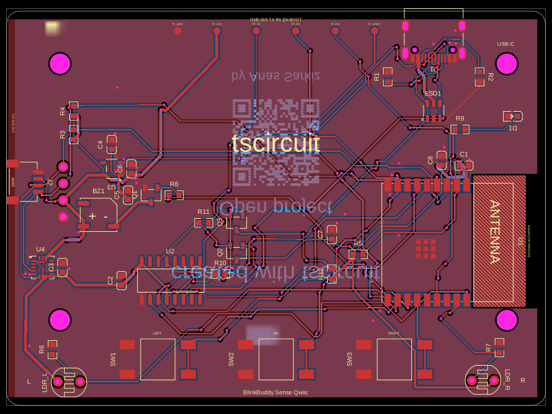 More from this authorAnasSarkiz/BlinkBuddyThis code defines and renders a 24mm square PCB silkscreen with a centered QR code graphic and labeling for open project instructions.
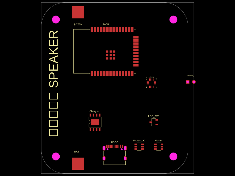 Similar packagemohan-bee/speakerThis code defines configurable 3D models and PCB footprints for various electronic components, including a battery charger IC, a dual Hall sensor, a dual power switch, and a voltage regulator, with detailed pinouts, footprints, and CAD models for schematic and physical design.
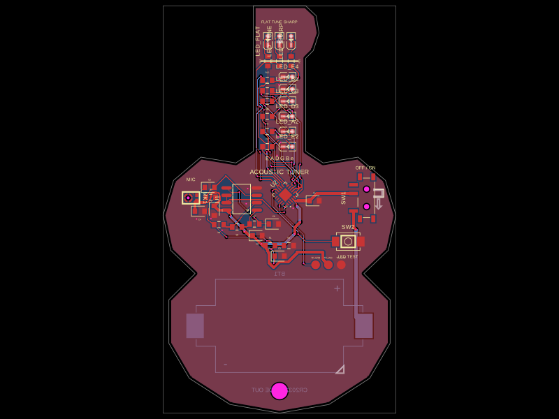 Discover something newgokul/acoustic-guitar-tunerThis code defines a miniature circuit board featuring a microcontroller (ATTINY1616-MNR), audio and power components, tactile switch, various LEDs, and passive components arranged with specific footprints, connections, and mechanical markings for a mini acoustic guitar tuner.