AnasSarkiz/ble-pedometer
This code defines and configures various electronic hardware components such as surface-mount resistors, crystals, diodes, transistors, connectors, and switches with their physical footprints, schematic symbols, and 3D CAD models for PCB assembly.
- Version
- 1.0.7
- License
- unset
- Stars
- 0
pcb-layout.ts
import type { ChipProps } from "@tscircuit/props"
import type { schematicLayout } from "./schematic-layout"

export const boardWidthMm = 60
export const boardHeightMm = 38

type ComponentName = keyof typeof schematicLayout
type PcbPlacement = Pick<ChipProps, "pcbX" | "pcbY" | "pcbRotation">

// Separate functional zones; do not scale footprints or RF/clock geometry.
// WSON charger perimeter pads replace the blocked ball-array escape.
export const pcbLayout = {
  J1_USB: { pcbX: -25.5, pcbY: -8, pcbRotation: 270 },
  J2_BATTERY: { pcbX: -24, pcbY: 14, pcbRotation: 180 },
  J3_DISPLAY: { pcbX: -4, pcbY: 14, pcbRotation: 180 },
  SW1_WAKE: { pcbX: -16, pcbY: -14 },
  R1_CC1: { pcbX: -21.3, pcbY: -3 },
  R2_CC2: { pcbX: -20, pcbY: -6.5 },
  D1_VBUS_TVS: { pcbX: -20, pcbY: -10 },
  C1_VBUS: { pcbX: -18.2, pcbY: 1.4 },

  U2_CHARGER: { pcbX: -15, pcbY: -2 },
  C2_VSYS: { pcbX: -18.4, pcbY: -3.5 },
  C3_BAT: { pcbX: -15.4, pcbY: -5.6 },
  U6_SYS_LDO: { pcbX: -9.5, pcbY: 0 },
  C5_LDO_IN: { pcbX: -10.5, pcbY: -3.8 },
  C6_SYS_VDD: { pcbX: -10.5, pcbY: 3, pcbRotation: 90 },
  R6_CE_PU: { pcbX: -11.5, pcbY: -5.3 },
  R7_PG_PU: { pcbX: -16.5, pcbY: -8.1 },
  R8_CHG_INT_PU: { pcbX: -14, pcbY: 1.5 },
  TP6_CHG_PG: { pcbX: -12, pcbY: -11 },

  U3_GAUGE: { pcbX: -20, pcbY: 8, pcbRotation: 180 },
  C7_GAUGE_BAT: { pcbX: -22.5, pcbY: 10.5 },
  C8_GAUGE_VDD: { pcbX: -17.5, pcbY: 7.6, pcbRotation: 90 },
  R9_BIN_PD: { pcbX: -16, pcbY: 5 },
  R10_GAUGE_INT_PU: { pcbX: -17, pcbY: 10.5 },

  U1_MCU: { pcbX: 18, pcbY: 5, pcbRotation: 180 },
  L1_DCDC: { pcbX: 12, pcbY: 3.5, pcbRotation: 180 },
  C9_VDDR_10U: { pcbX: 8, pcbY: 3.5 },
  C10_VDDR_100N_A: { pcbX: 21, pcbY: 8.8 },
  C11_VDDR_100N_B: { pcbX: 13.5, pcbY: -1 },
  C12_VDDD: { pcbX: 13.5, pcbY: 5.8, pcbRotation: 180 },
  C13_VDDS1: { pcbX: 17.25, pcbY: 9.5, pcbRotation: 90 },
  C14_VDDS2: { pcbX: 14.5, pcbY: 1.3, pcbRotation: 180 },
  C15_VDDS3: { pcbX: 19.2, pcbY: -2.5, pcbRotation: 270 },
  C16_VDDS_BULK: { pcbX: 19, pcbY: 12 },
  Y1_48MHZ: { pcbX: 17.7, pcbY: 0.5, pcbRotation: 270 },
  R11_RESET_PU: { pcbX: 14, pcbY: 8.5, pcbRotation: 180 },
  C17_RESET: { pcbX: 11.5, pcbY: 8.5 },

  U4_ACCEL: { pcbX: 20, pcbY: -6 },
  C18_ACCEL_VDD: { pcbX: 22.7, pcbY: -4.8 },
  C19_ACCEL_VDDIO: { pcbX: 22.7, pcbY: -7.3 },
  R12_I2C_SCL: { pcbX: 7, pcbY: 9 },
  R13_I2C_SDA: { pcbX: 7, pcbY: 6.5 },

  Q1_DISPLAY_SWITCH: { pcbX: -7, pcbY: 9.5, pcbRotation: 90 },
  R14_DISPLAY_GATE_PU: { pcbX: -10, pcbY: 10 },
  U5_DISPLAY_BUS_SWITCH: { pcbX: -1.5, pcbY: 9 },
  R15_DISPLAY_BUS_EN_PD: { pcbX: 2.5, pcbY: 8 },
  C20_DISPLAY_BULK: { pcbX: -9.5, pcbY: 14 },

  // Translate the reviewed MCU-to-antenna chain together to the new right edge.
  C21_RF_FILTER_IN: { pcbX: 21.55, pcbY: 1.2, pcbRotation: 270 },
  L2_RF_FILTER: { pcbX: 21.95, pcbY: 4.5 },
  C22_RF_FILTER_OUT: { pcbX: 22.4, pcbY: 6.6, pcbRotation: 90 },
  C23_RF_TUNE_IN: { pcbX: 23.1, pcbY: 2.3, pcbRotation: 270 },
  R16_RF_TUNE_SERIES: { pcbX: 24.05, pcbY: 4.5, pcbRotation: 90 },
  C24_RF_TUNE_OUT: { pcbX: 24, pcbY: 7.2, pcbRotation: 90 },
  ANT1: { pcbX: 27.7, pcbY: 4.5 },

  // SWD leaves the MCU's north edge; keep the fixture row on that same side.
  TP1_SWDIO: { pcbX: 14.4, pcbY: 15.5 },
  TP2_SWDCK: { pcbX: 16.6, pcbY: 15.5 },
  TP3_RESET: { pcbX: 18.8, pcbY: 15.5 },
  TP4_GND: { pcbX: 21, pcbY: 15.5 },
  TP5_SYS_VDD: { pcbX: 23.2, pcbY: 15.5 },
} satisfies Record<ComponentName, PcbPlacement>

export const antennaKeepoutPcbX = 27.4

// Inset copper from the new outline and preserve the antenna ground-plane notch.
export const groundPourOutline = [
  { x: -29.6, y: -18.6 },
  { x: 29.6, y: -18.6 },
  { x: 29.6, y: 0.6 },
  { x: 24.6, y: 0.6 },
  { x: 24.6, y: 7.8 },
  { x: 29.6, y: 7.8 },
  { x: 29.6, y: 18.6 },
  { x: -29.6, y: 18.6 },
]
Related Packages
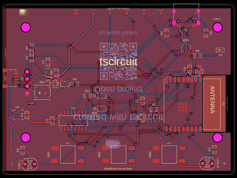 More from this authorAnasSarkiz/BlinkBuddyThis code defines and renders a 24mm square PCB silkscreen with a centered QR code graphic and labeling for open project instructions.
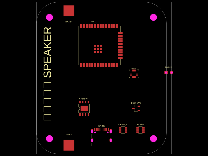 Similar packagemohan-bee/speakerThis code defines configurable 3D models and PCB footprints for various electronic components, including a battery charger IC, a dual Hall sensor, a dual power switch, and a voltage regulator, with detailed pinouts, footprints, and CAD models for schematic and physical design.
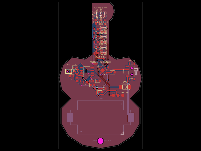 Discover something newgokul/acoustic-guitar-tunerThis code defines a miniature circuit board featuring a microcontroller (ATTINY1616-MNR), audio and power components, tactile switch, various LEDs, and passive components arranged with specific footprints, connections, and mechanical markings for a mini acoustic guitar tuner.