ShiboSoftwareDev/am625sip-linux-board
This code defines the physical footprint and pin layout for an AM625 System-in-Package (SIP) component, detailing pad positions, pin labels, and package outline for hardware integration.
- Version
- 1.0.24
- License
- unset
- Stars
- 0
subcircuits/cache/__snapshots__/usb0-analog-support.circuit-pcb.snap.svg
<svg xmlns="http://www.w3.org/2000/svg" width="800" height="600"><style></style><rect class="boundary" x="0" y="0" fill="#000" width="800" height="600" data-type="pcb_background" data-pcb-layer="global"/><rect class="pcb-boundary" fill="none" stroke="#fff" stroke-width="0.3" x="40" y="100" width="720" height="400" data-type="pcb_boundary" data-pcb-layer="global"/><path class="pcb-board" d="M 40 500 L 760 500 L 760 100 L 40 100 Z" fill="none" stroke="rgba(255, 255, 255, 0.5)" stroke-width="4" data-type="pcb_board" data-pcb-layer="board"/><path class="pcb-trace" stroke="rgb(255, 140, 0)" fill="none" d="M 203.99995349733996 300 L 120 300" stroke-width="12" stroke-linecap="round" stroke-linejoin="round" shape-rendering="crispEdges" data-type="pcb_trace" data-pcb-layer="inner1"/><path class="pcb-trace" stroke="rgb(255, 140, 0)" fill="none" d="M 120 300 L 120 300" stroke-width="12" stroke-linecap="round" stroke-linejoin="round" shape-rendering="crispEdges" data-type="pcb_trace" data-pcb-layer="inner1"/><rect class="pcb-pad" fill="rgb(200, 52, 52)" x="110" y="210" width="20" height="20" data-type="pcb_smtpad" data-pcb-layer="top"/><rect class="pcb-pad" fill="rgb(200, 52, 52)" x="110" y="370" width="20" height="20" data-type="pcb_smtpad" data-pcb-layer="top"/><rect class="pcb-pad" fill="rgb(200, 52, 52)" x="208.8" y="367.2" width="21.6" height="25.6" data-type="pcb_smtpad" data-pcb-layer="top"/><rect class="pcb-pad" fill="rgb(200, 52, 52)" x="249.59999999999997" y="367.2" width="21.6" height="25.6" data-type="pcb_smtpad" data-pcb-layer="top"/><rect class="pcb-pad" fill="rgb(200, 52, 52)" x="208.8" y="207.2" width="21.6" height="25.6" data-type="pcb_smtpad" data-pcb-layer="top"/><rect class="pcb-pad" fill="rgb(200, 52, 52)" x="249.59999999999997" y="207.2" width="21.6" height="25.6" data-type="pcb_smtpad" data-pcb-layer="top"/><rect class="pcb-pad" fill="rgb(200, 52, 52)" x="208.8" y="287.2" width="21.6" height="25.6" data-type="pcb_smtpad" data-pcb-layer="top"/><rect class="pcb-pad" fill="rgb(200, 52, 52)" x="249.59999999999997" y="287.2" width="21.6" height="25.6" data-type="pcb_smtpad" data-pcb-layer="top"/><rect class="pcb-pad" fill="rgb(200, 52, 52)" x="167.2" y="269.59999999999997" width="25.6" height="21.6" data-type="pcb_smtpad" data-pcb-layer="top"/><rect class="pcb-pad" fill="rgb(200, 52, 52)" x="167.2" y="228.79999999999998" width="25.6" height="21.6" data-type="pcb_smtpad" data-pcb-layer="top"/><rect class="pcb-pad" fill="rgb(200, 52, 52)" x="425.99944" y="246.001632" width="39.99992" height="31.999935999999998" data-type="pcb_smtpad" data-pcb-layer="top"/><rect class="pcb-pad" fill="rgb(200, 52, 52)" x="334.00064000000003" y="284.000032" width="39.99992" height="31.999935999999998" data-type="pcb_smtpad" data-pcb-layer="top"/><rect class="pcb-pad" fill="rgb(200, 52, 52)" x="425.99944" y="321.998432" width="39.99992" height="31.999935999999998" data-type="pcb_smtpad" data-pcb-layer="top"/><path class="pcb-trace" stroke="rgb(200, 52, 52)" fill="none" d="M 260.4 220 L 260.4 300" stroke-width="6" stroke-linecap="round" stroke-linejoin="round" shape-rendering="crispEdges" data-type="pcb_trace" data-pcb-layer="top"/><path class="pcb-trace" stroke="rgb(200, 52, 52)" fill="none" d="M 260.4 300 L 354 300" stroke-width="6" stroke-linecap="round" stroke-linejoin="round" shape-rendering="crispEdges" data-type="pcb_trace" data-pcb-layer="top"/><path class="pcb-trace" stroke="rgb(200, 52, 52)" fill="none" d="M 354 300 L 354.0006 300" stroke-width="6" stroke-linecap="round" stroke-linejoin="round" shape-rendering="crispEdges" data-type="pcb_trace" data-pcb-layer="top"/><path class="pcb-trace" stroke="rgb(200, 52, 52)" fill="none" d="M 180 280.4 L 219.60000000000002 240.79999999999998" stroke-width="6" stroke-linecap="round" stroke-linejoin="round" shape-rendering="crispEdges" data-type="pcb_trace" data-pcb-layer="top"/><path class="pcb-trace" stroke="rgb(200, 52, 52)" fill="none" d="M 219.60000000000002 240.79999999999998 L 219.60000000000002 220" stroke-width="6" stroke-linecap="round" stroke-linejoin="round" shape-rendering="crispEdges" data-type="pcb_trace" data-pcb-layer="top"/><path class="pcb-trace" stroke="rgb(200, 52, 52)" fill="none" d="M 120 220 L 180 280" stroke-width="6" stroke-linecap="round" stroke-linejoin="round" shape-rendering="crispEdges" data-type="pcb_trace" data-pcb-layer="top"/><path class="pcb-trace" stroke="rgb(200, 52, 52)" fill="none" d="M 180 280 L 180 280.4" stroke-width="6" stroke-linecap="round" stroke-linejoin="round" shape-rendering="crispEdges" data-type="pcb_trace" data-pcb-layer="top"/><path class="pcb-trace" stroke="rgb(200, 52, 52)" fill="none" d="M 120 380 L 219.60000000000002 380" stroke-width="6" stroke-linecap="round" stroke-linejoin="round" shape-rendering="crispEdges" data-type="pcb_trace" data-pcb-layer="top"/><path class="pcb-trace" stroke="rgb(200, 52, 52)" fill="none" d="M 219.60000000000002 300 L 203.99995349733996 300" stroke-width="12" stroke-linecap="round" stroke-linejoin="round" shape-rendering="crispEdges" data-type="pcb_trace" data-pcb-layer="top"/><path class="pcb-trace" stroke="rgb(200, 52, 52)" fill="none" d="M 120 300 L 120 300" stroke-width="12" stroke-linecap="round" stroke-linejoin="round" shape-rendering="crispEdges" data-type="pcb_trace" data-pcb-layer="top"/><path class="pcb-trace" stroke="rgb(200, 52, 52)" fill="none" d="M 445.9994 337.9984 L 445.9994 300" stroke-width="6" stroke-linecap="round" stroke-linejoin="round" shape-rendering="crispEdges" data-type="pcb_trace" data-pcb-layer="top"/><path class="pcb-trace" stroke="rgb(200, 52, 52)" fill="none" d="M 180 239.6 L 180 219.2" stroke-width="6" stroke-linecap="round" stroke-linejoin="round" shape-rendering="crispEdges" data-type="pcb_trace" data-pcb-layer="top"/><path class="pcb-trace" stroke="rgb(200, 52, 52)" fill="none" d="M 260.4 380 L 280.79999999999995 380" stroke-width="6" stroke-linecap="round" stroke-linejoin="round" shape-rendering="crispEdges" data-type="pcb_trace" data-pcb-layer="top"/><path class="pcb-trace" stroke="rgb(200, 52, 52)" fill="none" d="M 680 380 L 704.0912000000001 364" stroke-width="6" stroke-linecap="round" stroke-linejoin="round" shape-rendering="crispEdges" data-type="pcb_trace" data-pcb-layer="top"/><path class="pcb-silkscreen pcb-silkscreen-top" d="M 233.85435999999999 364.8 L 246.14564 364.8" fill="none" stroke="#f2eda1" stroke-width="4.8" stroke-linecap="round" stroke-linejoin="round" data-pcb-component-id="pcb_component_4" data-pcb-silkscreen-path-id="pcb_silkscreen_path_0" data-type="pcb_silkscreen_path" data-pcb-layer="top"/><path class="pcb-silkscreen pcb-silkscreen-top" d="M 233.85435999999999 395.2 L 246.14564 395.2" fill="none" stroke="#f2eda1" stroke-width="4.8" stroke-linecap="round" stroke-linejoin="round" data-pcb-component-id="pcb_component_4" data-pcb-silkscreen-path-id="pcb_silkscreen_path_1" data-type="pcb_silkscreen_path" data-pcb-layer="top"/><text x="0" y="0" dx="0" dy="0" fill="#f2eda1" font-family="Arial, sans-serif" font-size="16" text-anchor="middle" dominant-baseline="central" transform="matrix(1,0,0,1,240,331.2)" class="pcb-silkscreen-text pcb-silkscreen-top" data-pcb-silkscreen-text-id="pcb_silkscreen_text_0" stroke="none" data-type="pcb_silkscreen_text" data-pcb-layer="top">R26</text><path class="pcb-silkscreen pcb-silkscreen-top" d="M 233.85435999999999 204.8 L 246.14564 204.8" fill="none" stroke="#f2eda1" stroke-width="4.8" stroke-linecap="round" stroke-linejoin="round" data-pcb-component-id="pcb_component_5" data-pcb-silkscreen-path-id="pcb_silkscreen_path_2" data-type="pcb_silkscreen_path" data-pcb-layer="top"/><path class="pcb-silkscreen pcb-silkscreen-top" d="M 233.85435999999999 235.2 L 246.14564 235.2" fill="none" stroke="#f2eda1" stroke-width="4.8" stroke-linecap="round" stroke-linejoin="round" data-pcb-component-id="pcb_component_5" data-pcb-silkscreen-path-id="pcb_silkscreen_path_3" data-type="pcb_silkscreen_path" data-pcb-layer="top"/><text x="0" y="0" dx="0" dy="0" fill="#f2eda1" font-family="Arial, sans-serif" font-size="16" text-anchor="middle" dominant-baseline="central" transform="matrix(1,0,0,1,240,171.20000000000002)" class="pcb-silkscreen-text pcb-silkscreen-top" data-pcb-silkscreen-text-id="pcb_silkscreen_text_1" stroke="none" data-type="pcb_silkscreen_text" data-pcb-layer="top">R27</text><path class="pcb-silkscreen pcb-silkscreen-top" d="M 233.85435999999999 284.8 L 246.14564 284.8" fill="none" stroke="#f2eda1" stroke-width="4.8" stroke-linecap="round" stroke-linejoin="round" data-pcb-component-id="pcb_component_6" data-pcb-silkscreen-path-id="pcb_silkscreen_path_4" data-type="pcb_silkscreen_path" data-pcb-layer="top"/><path class="pcb-silkscreen pcb-silkscreen-top" d="M 233.85435999999999 315.2 L 246.14564 315.2" fill="none" stroke="#f2eda1" stroke-width="4.8" stroke-linecap="round" stroke-linejoin="round" data-pcb-component-id="pcb_component_6" data-pcb-silkscreen-path-id="pcb_silkscreen_path_5" data-type="pcb_silkscreen_path" data-pcb-layer="top"/><text x="0" y="0" dx="0" dy="0" fill="#f2eda1" font-family="Arial, sans-serif" font-size="16" text-anchor="middle" dominant-baseline="central" transform="matrix(1,0,0,1,240,251.2)" class="pcb-silkscreen-text pcb-silkscreen-top" data-pcb-silkscreen-text-id="pcb_silkscreen_text_2" stroke="none" data-type="pcb_silkscreen_text" data-pcb-layer="top">R28</text><path class="pcb-silkscreen pcb-silkscreen-top" d="M 164.8 266.14564 L 164.8 253.85435999999999" fill="none" stroke="#f2eda1" stroke-width="4.8" stroke-linecap="round" stroke-linejoin="round" data-pcb-component-id="pcb_component_7" data-pcb-silkscreen-path-id="pcb_silkscreen_path_6" data-type="pcb_silkscreen_path" data-pcb-layer="top"/><path class="pcb-silkscreen pcb-silkscreen-top" d="M 195.2 266.14564 L 195.2 253.85435999999999" fill="none" stroke="#f2eda1" stroke-width="4.8" stroke-linecap="round" stroke-linejoin="round" data-pcb-component-id="pcb_component_7" data-pcb-silkscreen-path-id="pcb_silkscreen_path_7" data-type="pcb_silkscreen_path" data-pcb-layer="top"/><text x="0" y="0" dx="0" dy="0" fill="#f2eda1" font-family="Arial, sans-serif" font-size="16" text-anchor="middle" dominant-baseline="central" transform="matrix(6.123233995736766e-17,-1,1,6.123233995736766e-17,131.2,260)" class="pcb-silkscreen-text pcb-silkscreen-top" data-pcb-silkscreen-text-id="pcb_silkscreen_text_3" stroke="none" data-type="pcb_silkscreen_text" data-pcb-layer="top">R29</text><path class="pcb-silkscreen pcb-silkscreen-top" d="M 372.0010720000005 274.5624079999999 L 372.0010720000005 240.00215200000014" fill="none" stroke="#f2eda1" stroke-width="4" stroke-linecap="round" stroke-linejoin="round" data-pcb-component-id="pcb_component_8" data-pcb-silkscreen-path-id="pcb_silkscreen_path_8" data-type="pcb_silkscreen_path" data-pcb-layer="top"/><path class="pcb-silkscreen pcb-silkscreen-top" d="M 372.0010720000005 240.00215200000014 L 412.00200800000005 240.00215200000014" fill="none" stroke="#f2eda1" stroke-width="4" stroke-linecap="round" stroke-linejoin="round" data-pcb-component-id="pcb_component_8" data-pcb-silkscreen-path-id="pcb_silkscreen_path_9" data-type="pcb_silkscreen_path" data-pcb-layer="top"/><path class="pcb-silkscreen pcb-silkscreen-top" d="M 428.00095999999996 312.56080800000007 L 428.00095999999996 287.44325600000025" fill="none" stroke="#f2eda1" stroke-width="4" stroke-linecap="round" stroke-linejoin="round" data-pcb-component-id="pcb_component_8" data-pcb-silkscreen-path-id="pcb_silkscreen_path_10" data-type="pcb_silkscreen_path" data-pcb-layer="top"/><path class="pcb-silkscreen pcb-silkscreen-top" d="M 372.0010720000005 360.0019120000002 L 372.0010720000005 325.4416560000004" fill="none" stroke="#f2eda1" stroke-width="4" stroke-linecap="round" stroke-linejoin="round" data-pcb-component-id="pcb_component_8" data-pcb-silkscreen-path-id="pcb_silkscreen_path_11" data-type="pcb_silkscreen_path" data-pcb-layer="top"/><path class="pcb-silkscreen pcb-silkscreen-top" d="M 372.0010720000005 360.0019120000002 L 412.00200800000005 360.0019120000002" fill="none" stroke="#f2eda1" stroke-width="4" stroke-linecap="round" stroke-linejoin="round" data-pcb-component-id="pcb_component_8" data-pcb-silkscreen-path-id="pcb_silkscreen_path_12" data-type="pcb_silkscreen_path" data-pcb-layer="top"/><text x="0" y="0" dx="0" dy="0" fill="#f2eda1" font-family="Arial, sans-serif" font-size="40" text-anchor="middle" dominant-baseline="central" transform="matrix(1,0,0,1,405.32892,200.1576)" class="pcb-silkscreen-text pcb-silkscreen-top" data-pcb-silkscreen-text-id="pcb_silkscreen_text_4" stroke="none" data-type="pcb_silkscreen_text" data-pcb-layer="top">D4</text><g data-type="pcb_plated_hole" data-pcb-layer="through"><circle class="pcb-hole-outer" fill="rgb(200, 52, 52)" cx="120" cy="300" r="16" data-type="pcb_plated_hole" data-pcb-layer="top"/><circle class="pcb-hole-inner" fill="#FF26E2" cx="120" cy="300" r="6" data-type="pcb_plated_hole_drill" data-pcb-layer="drill"/></g><g data-type="pcb_plated_hole" data-pcb-layer="through"><circle class="pcb-hole-outer" fill="rgb(200, 52, 52)" cx="680" cy="380" r="16" data-type="pcb_plated_hole" data-pcb-layer="top"/><circle class="pcb-hole-inner" fill="#FF26E2" cx="680" cy="380" r="6" data-type="pcb_plated_hole_drill" data-pcb-layer="drill"/></g><g data-type="pcb_via" data-pcb-layer="through"><circle class="pcb-hole-outer" fill="rgb(200, 52, 52)" cx="203.99995349733996" cy="300" r="4.8" data-type="pcb_via" data-pcb-layer="top"/><circle class="pcb-hole-inner" fill="#FF26E2" cx="203.99995349733996" cy="300" r="2" data-type="pcb_via" data-pcb-layer="drill"/></g><g data-type="pcb_via" data-pcb-layer="through"><circle class="pcb-hole-outer" fill="rgb(200, 52, 52)" cx="445.9994" cy="300" r="4.8" data-type="pcb_via" data-pcb-layer="top"/><circle class="pcb-hole-inner" fill="#FF26E2" cx="445.9994" cy="300" r="2" data-type="pcb_via" data-pcb-layer="drill"/></g><g data-type="pcb_via" data-pcb-layer="through"><circle class="pcb-hole-outer" fill="rgb(200, 52, 52)" cx="180" cy="219.2" r="4.8" data-type="pcb_via" data-pcb-layer="top"/><circle class="pcb-hole-inner" fill="#FF26E2" cx="180" cy="219.2" r="2" data-type="pcb_via" data-pcb-layer="drill"/></g><g data-type="pcb_via" data-pcb-layer="through"><circle class="pcb-hole-outer" fill="rgb(200, 52, 52)" cx="280.79999999999995" cy="380" r="4.8" data-type="pcb_via" data-pcb-layer="top"/><circle class="pcb-hole-inner" fill="#FF26E2" cx="280.79999999999995" cy="380" r="2" data-type="pcb_via" data-pcb-layer="drill"/></g><g data-type="pcb_via" data-pcb-layer="through"><circle class="pcb-hole-outer" fill="rgb(200, 52, 52)" cx="704.0912000000001" cy="364" r="4.8" data-type="pcb_via" data-pcb-layer="top"/><circle class="pcb-hole-inner" fill="#FF26E2" cx="704.0912000000001" cy="364" r="2" data-type="pcb_via" data-pcb-layer="drill"/></g></svg>Related Packages
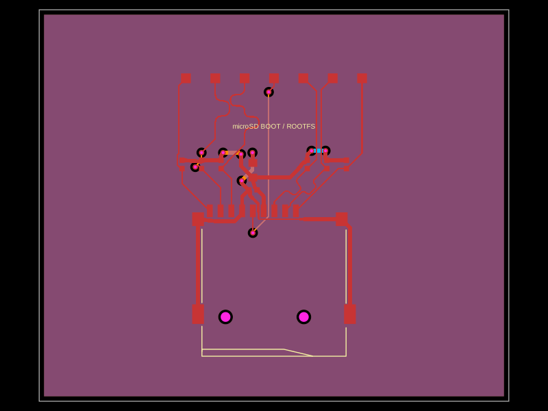 More from this authorShiboSoftwareDev/t113-s3-linux-computer-p9The code defines a PCB subcircuit for a buck converter module featuring a TMI3112H IC, FTC252010S power switch, and associated passive components like capacitors and resistors for voltage regulation and feedback control.
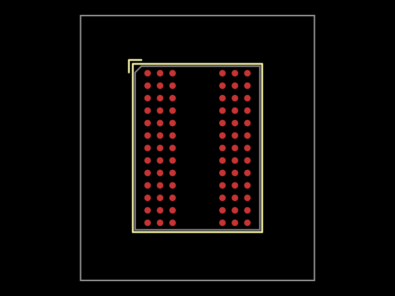 Similar package0hmX/mt41k512m8da-107-it-p-footprintsThis code defines the mechanical and physical layout of a Micron digital ball grid array (FBGA) package with 78 balls, including pin positions, footprint geometry, PCB pads, and silkscreen outlines for surface-mount integration.
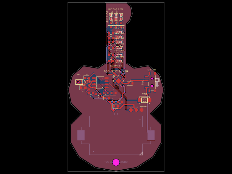 Discover something newgokul/acoustic-guitar-tunerThis code defines a miniature circuit board featuring a microcontroller (ATTINY1616-MNR), audio and power components, tactile switch, various LEDs, and passive components arranged with specific footprints, connections, and mechanical markings for a mini acoustic guitar tuner.