ShiboSoftwareDev/kicad-footprint
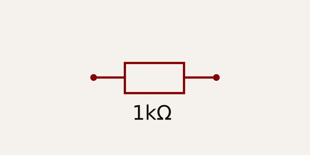
This code defines a grid of physical PCB elements including a 1kΩ resistor, various holes, pads, fiducials, cutouts, text labels, and annotation features for manufacturing and layout reference.
Usage: To import and use the "@tsci/ShiboSoftwareDev.kicad-footprint" package, follow these steps: 1. Import the component in your project: ```tsx import KicadFootprint from "@tsci/ShiboSoftwareDev.kicad-footprint" ``` 2. Use the component within a tscircuit board or panel: ```tsx <board> <KicadFootprint /> </board> ``` The package provides various PCB elements like resistors, breakout points, cutouts, fiducials, holes, SMT pads, and various note/text elements that can be used in circuit design.
- Version
- 0.0.1
- License
- unset
- Stars
- 0
dist/index.js
PCB

Schematic
import { jsxs, jsx } from 'react/jsx-runtime';

var index = () => (jsxs("panel", { layoutMode: "grid", children: [jsxs("board", { width: "10mm", height: "10mm", name: "B_breakout", children: [jsx("resistor", { name: "R1", resistance: "1k", footprint: "kicad:Resistor_SMD/R_0603_1608Metric" }), jsx("breakoutpoint", { connection: ".R1 > .pin1", pcbX: -2, pcbY: -2 })] }), jsx("board", { width: "10mm", height: "10mm", name: "B_cutout", children: jsx("cutout", { shape: "circle", radius: 1, pcbX: 0, pcbY: 0 }) }), jsx("board", { width: "10mm", height: "10mm", name: "B_fiducial", children: jsx("fiducial", { name: "F1", padDiameter: "1mm", pcbX: 0, pcbY: 0 }) }), jsx("board", { width: "10mm", height: "10mm", name: "B_hole", children: jsx("hole", { diameter: 1, pcbX: 0, pcbY: 0 }) }), jsx("board", { width: "10mm", height: "10mm", name: "B_platedhole", children: jsx("platedhole", { shape: "circle", outerDiameter: 2, holeDiameter: 1, pcbX: 0, pcbY: 0 }) }), jsx("board", { width: "10mm", height: "10mm", name: "B_smtpad", children: jsx("smtpad", { shape: "rect", width: 2, height: 2, pcbX: 0, pcbY: 0 }) }), jsx("board", { width: "10mm", height: "10mm", name: "B_pcbnotedimension", children: jsx("pcbnotedimension", { from: { x: -2, y: -2 }, to: { x: 2, y: 2 } }) }), jsx("board", { width: "10mm", height: "10mm", name: "B_pcbnotepath", children: jsx("pcbnotepath", { route: [
                    { x: -2, y: -2 },
                    { x: 2, y: 2 },
                ] }) }), jsx("board", { width: "10mm", height: "10mm", name: "B_coppertext", children: jsx("coppertext", { text: "Cu", pcbX: 0, pcbY: 0, fontSize: 1.5 }) }), jsx("board", { width: "10mm", height: "10mm", name: "B_pcbnoteline", children: jsx("group", { name: "g1 l1", children: jsx("pcbnoteline", { x1: -2, y1: -2, x2: 2, y2: 2 }) }) }), jsx("board", { width: "10mm", height: "10mm", name: "B_pcbnoterect", children: jsx("group", { name: "g2 l1", children: jsx("pcbnoterect", { width: 4, height: 4 }) }) }), jsx("board", { width: "10mm", height: "10mm", name: "B_pcbnotetext", children: jsx("group", { name: "g3 l1", children: jsx("group", { name: "g4 l2", children: jsx("pcbnotetext", { text: "Note" }) }) }) }), jsx("board", { width: "10mm", height: "10mm", name: "B_fabricationnotetext", children: jsx("fabricationnotetext", { text: "Fab Note" }) }), jsx("board", { width: "10mm", height: "10mm", name: "B_fabricationnoterect", children: jsx("fabricationnoterect", { width: 4, height: 4, strokeWidth: 0.2 }) }), jsx("board", { width: "10mm", height: "10mm", name: "B_fabricationnotepath", children: jsx("fabricationnotepath", { route: [
                    { x: -2, y: -2 },
                    { x: 2, y: 2 },
                ], strokeWidth: 0.1 }) }), jsx("board", { width: "10mm", height: "10mm", name: "B_fabricationnotedimension", children: jsx("fabricationnotedimension", { from: { x: -2, y: -2 }, to: { x: 2, y: 2 } }) })] }));

export { index as default };