ShiboSoftwareDev/t113-s3-linux-computer-p9
The code defines a PCB subcircuit for a buck converter module featuring a TMI3112H IC, FTC252010S power switch, and associated passive components like capacitors and resistors for voltage regulation and feedback control.
- Version
- 0.1.4
- License
- unset
- Stars
- 0
subcircuits/usb-power-frontend.tsx
import { Fragment } from "react"
import { C, R, cleanImportedSilk, part } from "../components/standard-passives"
import { ESD5Z5V0 } from "../imports/ESD5Z5V0"
import { MF_MSMF150_2 } from "../imports/MF_MSMF150_2"
import { TYPE_C_31_M_12 } from "../imports/TYPE_C_31_M_12"
import { USBLC6_2SC6 } from "../imports/USBLC6_2SC6"

const SECTION = "POWER_INPUT"
const throughViaLayers = ["top", "inner1", "inner2", "inner3", "inner4", "inner5", "inner6", "inner7", "inner8", "bottom"] as const
const groundFanoutPhases = Array.from({ length: 12 }, (_, index) => -40 + index)

export const UsbPowerFrontend = () => (
  <subcircuit
    name="USB_POWER_FRONTEND"
    pcbX={-18}
    pcbY={-4}
    width="34mm"
    height="26mm"
    autorouter="default"
    autorouterVersion="beta_pipeline9"
    autorouterEffortLevel="10x"
    defaultTraceWidth="0.15mm"
    exposeNets
  >
    <net name="GND" isGroundNet routingPhaseIndex={-40} nominalTraceWidth="0.30mm" />
    {groundFanoutPhases.map((phaseIndex) => <Fragment key={`usb-ground-fanout-${phaseIndex}`}>
      <autoroutingphase name={`USB_GROUND_FANOUT_${phaseIndex}`} phaseIndex={phaseIndex} autorouter="fanout"
        fanoutBoundaryPadding="4mm" fanoutRoutingLayers={[...throughViaLayers]}
        fanoutPourNetMap={{ inner5: "GND" }} />
    </Fragment>)}
    <TYPE_C_31_M_12
      {...cleanImportedSilk}
      name="J_USB_C"
      pcbX={-7}
      pcbY={-7.5}
      noConnect={["B8", "A8"]}
      schSectionName={SECTION}
    />
    <MF_MSMF150_2 {...cleanImportedSilk} name="F_VBUS" pcbX={1.5} pcbY={-5.3} schSectionName={SECTION} />
    <ESD5Z5V0 {...cleanImportedSilk} name="D_VBUS_TVS" pcbX={8.2} pcbY={-8} schSectionName={SECTION} />
    <C name="C_VBUS_BULK_A" capacitance={part.c22u.value} mpn={part.c22u.mpn} lcsc={part.c22u.lcsc}
      size="0603" x={9} y={-5} rotation={90} sectionName={SECTION} />
    <C name="C_VBUS_BULK_B" capacitance={part.c22u.value} mpn={part.c22u.mpn} lcsc={part.c22u.lcsc}
      size="0603" x={11.5} y={-5} rotation={90} sectionName={SECTION} />
    <R name="R_USB_CC1" resistance={part.r5k1.value} mpn={part.r5k1.mpn} lcsc={part.r5k1.lcsc}
      x={-9.5} y={-3} rotation={90} sectionName={SECTION} />
    <R name="R_USB_CC2" resistance={part.r5k1.value} mpn={part.r5k1.mpn} lcsc={part.r5k1.lcsc}
      x={-4.5} y={-3} rotation={90} sectionName={SECTION} />
    <R name="R_USB_DM_BRIDGE" resistance={part.r0.value} mpn={part.r0.mpn} lcsc={part.r0.lcsc}
      x={-7.25} y={-4} sectionName={SECTION} />
    <R name="R_USB_DP_BRIDGE" resistance={part.r0.value} mpn={part.r0.mpn} lcsc={part.r0.lcsc}
      x={-6.75} y={-2.5} sectionName={SECTION} />
    <USBLC6_2SC6 {...cleanImportedSilk} name="U_USB_ESD" pcbX={-7} pcbY={2} pcbRotation={0} schSectionName={SECTION} />
    <testpoint name="TP_USB_DP" pcbX={-8} pcbY={7.5}
      footprint={<footprint><smtpad portHints={["pin1"]} pcbX={0} pcbY={0} shape="circle" radius="0.5mm" /><courtyardcircle pcbX={0} pcbY={0} radius="0.7mm" /></footprint>}
      connections={{ pin1: "net.USB0_DP" }} schSectionName={SECTION} />
    <testpoint name="TP_USB_DM" pcbX={-6} pcbY={7.5}
      footprint={<footprint><smtpad portHints={["pin1"]} pcbX={0} pcbY={0} shape="circle" radius="0.5mm" /><courtyardcircle pcbX={0} pcbY={0} radius="0.7mm" /></footprint>}
      connections={{ pin1: "net.USB0_DM" }} schSectionName={SECTION} />

    <trace name="USB_VBUS_A_IN" from="J_USB_C.A4B9" to="F_VBUS.pin1"
      width="0.8mm" routingPhaseIndex={-90} />
    <trace name="USB_VBUS_B_IN" from="J_USB_C.B4A9" to="F_VBUS.pin1"
      width="0.8mm" routingPhaseIndex={-89} />
    <trace name="VBUS_FUSED" from="F_VBUS.pin2" to="net.VBUS_5V" width="0.8mm" />
    <trace name="VBUS_TVS" from="D_VBUS_TVS.C" to="net.VBUS_5V" width="0.6mm" />
    <trace name="VBUS_TVS_GROUND" from="D_VBUS_TVS.A" to="net.GND" width="0.4mm" routingPhaseIndex={-40} />
    <trace name="VBUS_BULK_A" from="C_VBUS_BULK_A.pin1" to="net.VBUS_5V" width="0.7mm" />
    <trace name="VBUS_BULK_A_GROUND" from="C_VBUS_BULK_A.pin2" to="net.GND" width="0.4mm" routingPhaseIndex={-39} />
    <trace name="VBUS_BULK_B" from="C_VBUS_BULK_B.pin1" to="net.VBUS_5V" width="0.7mm" />
    <trace name="VBUS_BULK_B_GROUND" from="C_VBUS_BULK_B.pin2" to="net.GND" width="0.4mm" routingPhaseIndex={-38} />

    <trace name="USB_GROUND_A" from="J_USB_C.A1B12" to="net.GND" width="0.3mm" routingPhaseIndex={-37} />
    <trace name="USB_GROUND_B" from="J_USB_C.B1A12" to="net.GND" width="0.3mm" routingPhaseIndex={-36} />
    <trace name="USB_SHELL_EH1" from="J_USB_C.EH1" to="net.GND" width="0.3mm" routingPhaseIndex={-35} />
    <trace name="USB_SHELL_EH2" from="J_USB_C.EH2" to="net.GND" width="0.3mm" routingPhaseIndex={-34} />
    <trace name="USB_SHELL_EH3" from="J_USB_C.EH3" to="net.GND" width="0.3mm" routingPhaseIndex={-33} />
    <trace name="USB_SHELL_EH4" from="J_USB_C.EH4" to="net.GND" width="0.3mm" routingPhaseIndex={-32} />
    <trace name="USB_CC1" from="J_USB_C.A5" to="R_USB_CC1.pin1" routingPhaseIndex={-88} />
    <trace name="USB_CC1_GROUND" from="R_USB_CC1.pin2" to="net.GND" routingPhaseIndex={-31} />
    <trace name="USB_CC2" from="J_USB_C.B5" to="R_USB_CC2.pin1" routingPhaseIndex={-87} />
    <trace name="USB_CC2_GROUND" from="R_USB_CC2.pin2" to="net.GND" routingPhaseIndex={-30} />

    <trace name="USB_B7_ESCAPE" from="J_USB_C.B7" to="R_USB_DM_BRIDGE.pin1"
      maxLength="12mm" maxViaCount={2} routingPhaseIndex={-77} />
    <trace name="USB_B6_ESCAPE" from="J_USB_C.B6" to="R_USB_DP_BRIDGE.pin2"
      maxLength="12mm" maxViaCount={2} routingPhaseIndex={-78} />
    <trace name="USB_DP_A_TO_ESD" path={["J_USB_C.A6", "R_USB_DP_BRIDGE.pin1", "U_USB_ESD.pin1"]}
      maxLength="20mm" maxViaCount={2} routingPhaseIndex={-75} />
    <trace name="USB_DM_A_TO_ESD" path={["J_USB_C.A7", "R_USB_DM_BRIDGE.pin2", "U_USB_ESD.pin3"]}
      maxLength="20mm" maxViaCount={2} routingPhaseIndex={-76} />
    <trace name="USB_DP_PROTECTED" from="U_USB_ESD.pin6" to="TP_USB_DP.pin1"
      maxLength="12mm" maxViaCount={0} routingPhaseIndex={-64} />
    <trace name="USB_DM_PROTECTED" from="U_USB_ESD.pin4" to="TP_USB_DM.pin1"
      maxLength="12mm" maxViaCount={0} routingPhaseIndex={-63} />
    <trace name="USB_ESD_GROUND" from="U_USB_ESD.GND" to="net.GND" width="0.4mm" routingPhaseIndex={-29} />
    <trace name="USB_ESD_VBUS" from="U_USB_ESD.VBUS" to="net.VBUS_5V" width="0.4mm" />

    <silkscreentext text="USB-C 5V INPUT + USB0 FEL" pcbX={-3.5} pcbY={-12} fontSize="0.65mm" />
  </subcircuit>
)
Related Packages
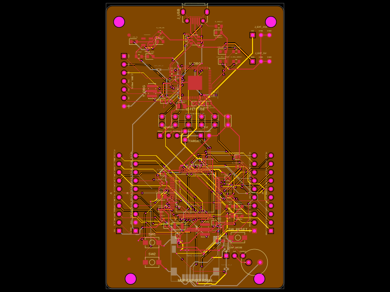 More from this authorShiboSoftwareDev/msp-exp430fr5994This code defines and renders electronic components such as a 4MHz ceramic resonator and various microcontroller chips with their physical pin layouts footprints, 3D models, and associated metadata.
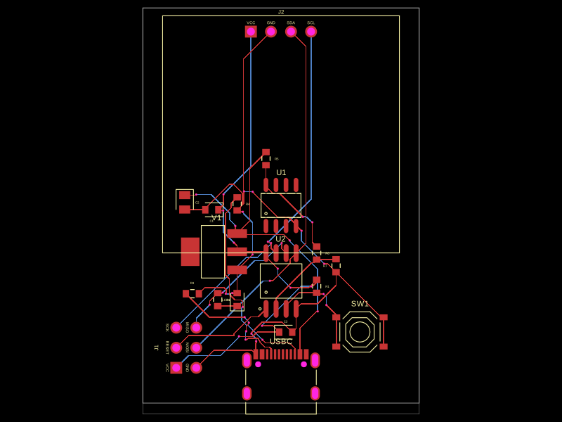 Similar packagemohan-bee/temperature-meterThe code defines a compact PCB assembly featuring a USB-C power input, an AMS1117 voltage regulator, a LM335 temperature sensor, an ATtiny85 microcontroller with ICSP and I2C headers, a pushbutton, and associated passive components like resistors and capacitors, all interconnected with traces and mounted on labeled footprints.
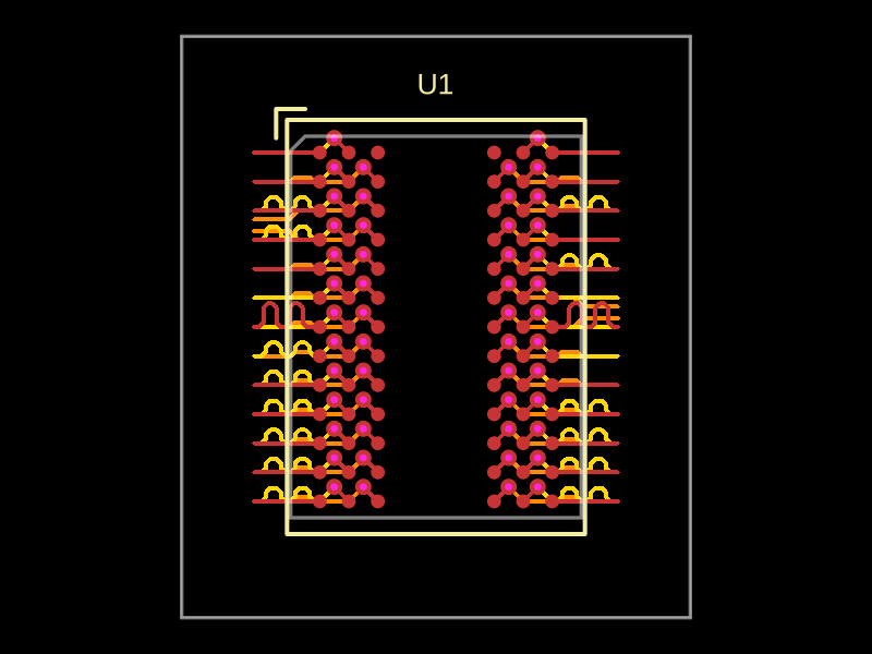 Discover something new0hmX/mt41k512m8da-107-it-p-fanoutThis code defines the physical footprint, routing, and layout configuration for a DDR3 memory module using surface-mount pads, vias, and copper traces on a printed circuit board (PCB).