astra/f1c100s
The code defines the physical pin layout, labels, and footprint for the F1C100S system-on-chip (SoC) component used in electronic devices.
- Version
- 0.9.2
- License
- unset
- Stars
- 0
scripts/check-plated-exits.ts
import type { CircuitJson } from "circuit-json";
import { EXTERNAL_NETS } from "../src/pin-map";
import { EXIT_DIAMETER, EXIT_DRILL } from "../src/profiles";

/** Check the emitted plated barrels and routing ports, not just JSX props. */
export function checkPlatedExits(
	json: CircuitJson,
	expected = EXTERNAL_NETS.length,
): string[] {
	const data = json as any[],
		errors: string[] = [];
	const sources = data.filter(
		(e) => e.type === "source_component" && e.ftype === "simple_test_point",
	);
	const holes = data.filter((e) => e.type === "pcb_plated_hole");
	if (sources.length !== expected || holes.length !== expected)
		errors.push(`Expected ${expected} plated breakout test points`);
	let innerLayerExits = 0;
	for (const source of sources) {
		const component = data.find(
			(e) =>
				e.type === "pcb_component" &&
				e.source_component_id === source.source_component_id,
		);
		const pads = holes.filter(
			(e) => e.pcb_component_id === component?.pcb_component_id,
		);
		const ports = data.filter(
			(e) =>
				e.type === "pcb_port" &&
				e.pcb_component_id === component?.pcb_component_id,
		);
		if (pads.length !== 1 || ports.length !== 1) {
			errors.push(`${source.name}: expected one barrel and port`);
			continue;
		}
		const h = pads[0],
			p = ports[0];
		if (
			h.outer_diameter !== EXIT_DIAMETER ||
			h.hole_diameter !== EXIT_DRILL ||
			h.is_covered_with_solder_mask ||
			!component.do_not_place
		)
			errors.push(`${source.name}: incorrect exposed test-point geometry`);
		for (const item of [h, p])
			if (
				["top", "inner1", "inner2", "bottom"].some(
					(layer) => !item.layers.includes(layer),
				)
			)
				errors.push(`${source.name}: missing layer access`);
		if (
			data.some(
				(e) =>
					e.type === "pcb_smtpad" &&
					e.pcb_component_id === component.pcb_component_id,
			)
		)
			errors.push(`${source.name}: old surface pad remains`);
		if (
			data.some(
				(e) => e.type === "pcb_via" && Math.hypot(e.x - h.x, e.y - h.y) < 1e-6,
			)
		)
			errors.push(`${source.name}: redundant coincident via`);
		const contacts = data
			.filter((e) => e.type === "pcb_trace")
			.flatMap((t) => [t.route[0], t.route.at(-1)])
			.filter((p) => Math.hypot(p.x - h.x, p.y - h.y) < 1e-5);
		if (!contacts.length) errors.push(`${source.name}: no routed contact`);
		if (contacts.some((p) => p.layer !== "top")) innerLayerExits++;
	}
	if (!innerLayerExits)
		errors.push("No saved bus routes arrive on a non-top layer");
	return errors;
}
Related Packages
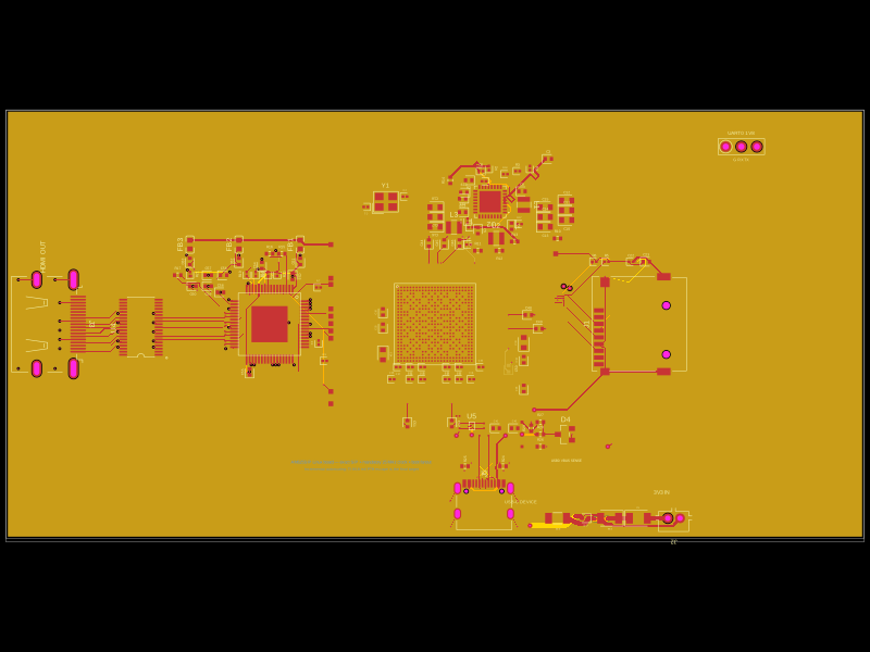 Similar packageShiboSoftwareDev/am625sip-linux-boardThis code defines the physical footprint and pin layout for an AM625 System-in-Package (SIP) component, detailing pad positions, pin labels, and package outline for hardware integration.
 Discover something newMustafaMulla29/wireless-mouse-pcbThis code defines a 3.3V low dropout voltage regulator chip (AP2112K-3.3TRG1) with five pins (VIN, GND, Enable, NC, VOUT) and its associated PCB footprint and 3D models for hardware implementation.