0hmX/am62l-lpddr4-clean
This code defines the hardware connections and routing logic for a DDR memory interface, specifying physical signal mappings between the system-on-chip (SoC) and DDR memory components, including connections for data, address, clock, reset, and power/ground balls.
- Version
- 1.0.0
- License
- unset
- Stars
- 0
index.circuit.tsx
PCB
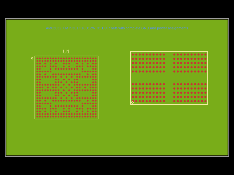
Schematic

import { Fragment } from "react"
import { DDR_CONNECTIONS, tracesFor } from "./ddr-connections"
import { Dram, Soc } from "./memory-components"
import {
  DRAM_GROUND_BALLS,
  DRAM_VDD1_BALLS,
  DRAM_VDD2_BALLS,
  DRAM_VDDQ_BALLS,
  SOC_DDR_POWER_BALLS,
  SOC_GROUND_BALLS,
} from "./power-balls"

const buses = [
  { name: "DDR_BYTE0", layers: ["top", "inner4"], skew: 8 },
  { name: "DDR_BYTE1", layers: ["inner5", "bottom"], skew: 14.5 },
  { name: "DDR_ADDR_CTRL", layers: ["inner6"], skew: 15 },
  { name: "DDR_CLOCK", layers: ["inner5"], skew: 0.25 },
  { name: "DDR_DQS0", layers: ["inner5"], skew: 0.25 },
  { name: "DDR_DQS1", layers: ["inner5"], skew: 0.25 },
  { name: "DDR_RESET", layers: ["inner6"] },
] as const

export default () => (
  <board
    name="AM62L32_LPDDR4_CLEAN"
    width="42mm"
    height="26mm"
    layers={8}
    defaultTraceWidth="0.08128mm"
    minTraceWidth="0.08128mm"
    minTraceToPadEdgeClearance="0.05mm"
    minViaEdgeToPadEdgeClearance="0.08128mm"
    minViaHoleEdgeToViaHoleEdgeClearance="0.1016mm"
    minViaHoleDiameter="0.1mm"
    minViaPadDiameter="0.24mm"
    pcbStyle={{ viaHoleDiameter: "0.1mm", viaPadDiameter: "0.24mm" }}
    allowBlindAndBuriedVias={false}
    isViaInPadAllowed={false}
    routingDisabled
  >
    <copperpour layer="inner1" connectsTo="net.GND" />
    <copperpour layer="inner2" connectsTo="net.VDD_LPDDR4" />
    <copperpour layer="inner3" connectsTo="net.SOC_DVDD1V8" />

    {buses.map((bus) => (
      <Fragment key={bus.name}>
        <bus
          name={bus.name}
          connections={tracesFor(bus.name)}
          preferredLayers={[...bus.layers]}
          maxLengthSkew={"skew" in bus ? bus.skew : undefined}
        />
      </Fragment>
    ))}

    <differentialpair
      name="DDR_CLOCK_PAIR"
      positiveConnection="CK_t"
      negativeConnection="CK_c"
      maxLengthSkew={0.25}
    />
    <differentialpair
      name="DDR_DQS0_PAIR"
      positiveConnection="DQS0_t"
      negativeConnection="DQS0_c"
      maxLengthSkew={0.25}
    />
    <differentialpair
      name="DDR_DQS1_PAIR"
      positiveConnection="DQS1_t"
      negativeConnection="DQS1_c"
      maxLengthSkew={0.25}
    />

    <breakout
      name="SOC_FANOUT"
      pcbX={-9.5}
      padding="3mm"
    >
      <Soc />

      <trace name="U1_GND_PLANE_DROP" from=".U1 > .A1" to="net.GND" />
      <trace
        name="U1_VDD_LPDDR4_PLANE_DROP"
        from=".U1 > .L8"
        to="net.VDD_LPDDR4"
      />
    </breakout>

    <breakout
      name="DRAM_FANOUT"
      pcbX={9.8}
      pcbY={1.81916}
      padding="3mm"
    >
      <Dram />

      <trace name="U2_GND_PLANE_DROP" from=".U2 > .A3" to="net.GND" />
      <trace
        name="U2_VDDQ_PLANE_DROP"
        from=".U2 > .B3"
        to="net.VDD_LPDDR4"
      />
      <trace
        name="U2_VDD2_PLANE_DROP"
        from=".U2 > .A4"
        to="net.VDD_LPDDR4"
      />
      <trace
        name="U2_VDD1_PLANE_DROP"
        from=".U2 > .F1"
        to="net.SOC_DVDD1V8"
      />
    </breakout>

    <group name="POWER_ASSIGNMENTS" routingDisabled>
      {SOC_GROUND_BALLS.filter((ball) => ball !== "A1").map((ball) => (
        <Fragment key={`U1-GND-${ball}`}>
          <trace name={`U1_GND_${ball}`} from={`U1.${ball}`} to="net.GND" />
        </Fragment>
      ))}
      {SOC_DDR_POWER_BALLS.filter((ball) => ball !== "L8").map((ball) => (
        <Fragment key={`U1-VDD-${ball}`}>
          <trace
            name={`U1_VDD_LPDDR4_${ball}`}
            from={`U1.${ball}`}
            to="net.VDD_LPDDR4"
          />
        </Fragment>
      ))}
      {DRAM_GROUND_BALLS.filter((ball) => ball !== "A3").map((ball) => (
        <Fragment key={`U2-GND-${ball}`}>
          <trace name={`U2_GND_${ball}`} from={`U2.${ball}`} to="net.GND" />
        </Fragment>
      ))}
      {DRAM_VDDQ_BALLS.filter((ball) => ball !== "B3").map((ball) => (
        <Fragment key={`U2-VDDQ-${ball}`}>
          <trace
            name={`U2_VDDQ_${ball}`}
            from={`U2.${ball}`}
            to="net.VDD_LPDDR4"
          />
        </Fragment>
      ))}
      {DRAM_VDD2_BALLS.filter((ball) => ball !== "A4").map((ball) => (
        <Fragment key={`U2-VDD2-${ball}`}>
          <trace
            name={`U2_VDD2_${ball}`}
            from={`U2.${ball}`}
            to="net.VDD_LPDDR4"
          />
        </Fragment>
      ))}
      {DRAM_VDD1_BALLS.filter((ball) => ball !== "F1").map((ball) => (
        <Fragment key={`U2-VDD1-${ball}`}>
          <trace
            name={`U2_SOC_DVDD1V8_${ball}`}
            from={`U2.${ball}`}
            to="net.SOC_DVDD1V8"
          />
        </Fragment>
      ))}
    </group>

    {DDR_CONNECTIONS.map((connection) => (
      <Fragment key={connection.trace}>
        <trace
          name={connection.trace}
          from={`U1.${connection.socSignal}`}
          to={`U2.${connection.memorySignal}`}
        />
      </Fragment>
    ))}

    <pcbnotetext
      pcbX={0}
      pcbY={11.2}
      fontSize="0.65mm"
      text="AM62L32 + MT53E1G16D1ZW: 31 DDR nets with complete GND and power assignments"
    />
  </board>
)