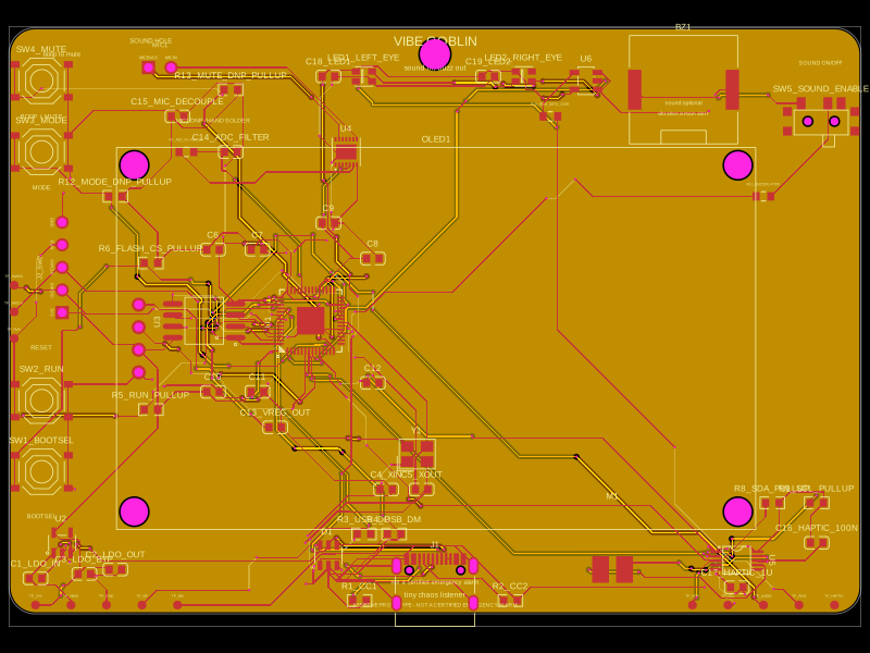
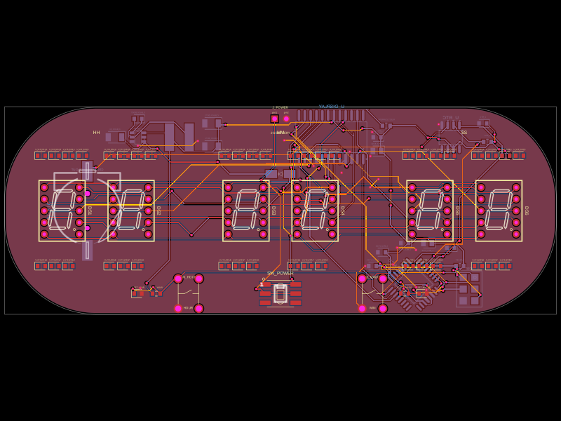
This code defines a PCB layout featuring a voltage probe module with key components including an RP2040 microcontroller, resistors, LEDs, connectors, and a custom probe interface, along with their physical footprints and routing details.
# VoltPeek Probe

VoltPeek Probe is a small 2-layer handheld DC voltage probe board. It accepts a plug-in 3.5 mm probe cable, divides a 0-12 V DC input down to a 3.3 V-safe ADC range, and presents the measurement path to a XIAO-style MCU module that can drive a 0.96 inch SSD1306 I2C OLED.

## Use

Use a probe cable with the red probe tip connected to the 3.5 mm plug TIP and the black alligator ground clip connected to SLEEVE. Clip ground to the target PCB first, then touch the red probe to the voltage node. The board is for 0-12 V DC only.

Do not use this board for mains voltage, high voltage, or AC measurement.

## Probe Jack Pinout

The selected jack is SHOU HAN PJ-320D, LCSC/JLCPCB C431535. Its LCSC datasheet labels the contacts as 0A, 0B, 0C, and 0D rather than TIP/RING/SLEEVE. Based on the datasheet mechanical contact order with the plug entering from the board edge:

- TIP = terminal 0D = imported `.J1 > .pin2` = `VIN_PROBE`
- RING = terminal 0C = imported `.J1 > .pin3` = NC
- SLEEVE/GND = terminal 0B and terminal 0A = imported `.J1 > .pin4` and `.J1 > .pin1` = `GND`

Assumption to check before fabrication: verify the PJ-320D terminal-to-plug mapping with a continuity meter on one sample jack and the intended TRS probe plug.

## Voltage Divider

The raw probe input never connects directly to the MCU ADC.

`Vadc = Vin * 33k / (100k + 33k)`

At `Vin = 12 V`, `Vadc` is about `2.98 V`. R3 is a 1 k series resistor between `ADC_DIV` and the MCU `ADC_SENSE` pin.

## Assembly

All components are on the top side. The bottom side is reserved for traces, vias, copper pour, and silkscreen only.

JLCPCB/LCSC assembled candidates:

| Ref | Part | LCSC/JLCPCB | Notes |
| --- | --- | --- | --- |
| R1 | 100 k 0603 resistor | C25803 | VIN_PROBE to ADC_DIV |
| R2 | 33 k 0603 resistor | C4216 | ADC_DIV to GND |
| R3 | 1 k 0603 resistor | C21190 | ADC series resistor |
| R4 | 330 ohm 0603 resistor | C23138 | LED current limit |
| R5 | 10 k 0603 resistor | C25804 | BUTTON_MODE pull-up |
| D1 | Green 0603 LED | C965805 | Status LED |
| SW1 | Tactile switch | C240290 | HOLD/MIN/MAX mode button |
| J1 | PJ-320D 3.5 mm audio jack | C431535 | Probe jack, top side |
| J2 | 4-pin 2.54 mm header/socket | C5144876 | OLED VCC/GND/SDA/SCL |

Hand-soldered/DNP items:

| Ref | Part | Notes |
| --- | --- | --- |
| U1 | Seeed Studio XIAO RP2040 module | Hand-soldered module or sockets. USB/programming stays on the module. |
| OLED | 0.96 inch SSD1306 I2C OLED module | Hand-soldered to J2. Confirm pin order is VCC, GND, SDA, SCL before plugging in. |

## Electrical Checklist

- Probe TIP connects to `VIN_PROBE`.
- Probe SLEEVE connects to `GND`.
- `VIN_PROBE` reaches `ADC_DIV` only through R1.
- R2 ties `ADC_DIV` to `GND`.
- R3 connects `ADC_DIV` to `ADC_SENSE`.
- The MCU ADC reads `ADC_SENSE`, not raw `VIN_PROBE`.
- OLED uses `VCC_3V3`, `GND`, `OLED_SDA`, and `OLED_SCL`.
- Button has a 10 k pull-up to `VCC_3V3` and shorts `BUTTON_MODE` to `GND` when pressed.
- LED is driven through R4 before D1 to `GND`.
- Top and bottom GND copper pours are included.

## Fabrication Assumptions To Verify

- Confirm the PJ-320D contact mapping against the exact plug cable before ordering.
- Confirm the XIAO module pinout and orientation match the chosen module variant.
- Confirm the OLED module pin order is VCC, GND, SDA, SCL and that it accepts 3.3 V logic and supply.
- Confirm JLCPCB assembly availability for imported connector/switch and selected headers at order time.