AnasSarkiz/VoltPeek
This code defines a PCB layout featuring a voltage probe module with key components including an RP2040 microcontroller, resistors, LEDs, connectors, and a custom probe interface, along with their physical footprints and routing details.
- Version
- 1.0.0
- License
- unset
- Stars
- 0
imports/TAC_32N_Q_T_R.tsx
import type { ChipProps } from "@tscircuit/props"

const pinLabels = {
  pin1: ["pin1"],
  pin2: ["pin2"],
  pin3: ["pin3"],
  pin4: ["pin4"],
  pin5: ["pin5"],
  pin6: ["pin6"]
} as const

export const TAC_32N_Q_T_R = (props: ChipProps<typeof pinLabels>) => {
  return (
    <chip
      pinLabels={pinLabels}
      supplierPartNumbers={{
  "jlcpcb": [
    "C240290"
  ]
}}
      manufacturerPartNumber="TAC_32N_Q_T_R"
      footprint={<footprint>
        <platedhole  portHints={["pin6"]} pcbX="3.499993mm" pcbY="-0.9999218mm" outerDiameter="1.1999976mm" holeDiameter="0.7999984mm" shape="circle" />
<platedhole  portHints={["pin5"]} pcbX="-3.499993mm" pcbY="-0.9999218mm" outerDiameter="1.1999976mm" holeDiameter="0.7999984mm" shape="circle" />
<smtpad portHints={["pin4"]} pcbX="2.499995mm" pcbY="-2.3999698mm" width="0.999998mm" height="0.7999984mm" shape="rect" />
<smtpad portHints={["pin3"]} pcbX="-2.499995mm" pcbY="-2.3999698mm" width="0.999998mm" height="0.7999984mm" shape="rect" />
<smtpad portHints={["pin2"]} pcbX="2.499995mm" pcbY="2.1999702mm" width="0.999998mm" height="1.1999976mm" shape="rect" />
<smtpad portHints={["pin1"]} pcbX="-2.499995mm" pcbY="2.1999702mm" width="0.999998mm" height="1.1999976mm" shape="rect" />
<silkscreenpath route={[{"x":3.6500053999999977,"y":-1.8173699999999826},{"x":3.6500053999999977,"y":-2.0999957999999737},{"x":3.2310070000000053,"y":-2.0999957999999737}]} />
<silkscreenpath route={[{"x":-3.6499799999999993,"y":-0.18247359999999446},{"x":-3.6499799999999993,"y":1.3999972000000156},{"x":3.6500053999999977,"y":1.3999972000000156},{"x":3.6500053999999977,"y":-0.18247359999999446}]} />
<silkscreenpath route={[{"x":-3.2312609999999893,"y":-2.0999957999999737},{"x":-3.6499799999999993,"y":-2.0999957999999737},{"x":-3.6499799999999993,"y":-1.8173699999999826}]} />
<silkscreenpath route={[{"x":-1.5001239999999996,"y":-3.599916599999986},{"x":-1.4999969999999792,"y":-2.0999957999999737}]} />
<silkscreenpath route={[{"x":1.4998700000000156,"y":-3.599916599999986},{"x":1.4999970000000076,"y":-2.0999957999999737}]} />
<silkscreenpath route={[{"x":-1.4999969999999792,"y":-3.5998657999999892},{"x":1.4997429999999952,"y":-3.5998657999999892}]} />
<silkscreenpath route={[{"x":-1.7689829999999915,"y":-2.0999957999999737},{"x":1.7687290000000075,"y":-2.0999957999999737}]} />
<silkscreentext text="{NAME}" pcbX="0.0057658mm" pcbY="3.797556mm" anchorAlignment="center" fontSize="1mm" />
<courtyardoutline outline={[{"x":-4.397134199999996,"y":3.0475560000000144},{"x":4.408665799999994,"y":3.0475560000000144},{"x":4.408665799999994,"y":-3.95484399999998},{"x":-4.397134199999996,"y":-3.95484399999998},{"x":-4.397134199999996,"y":3.0475560000000144}]} />
      </footprint>}
      cadModel={{
        objUrl: "https://modelcdn.tscircuit.com/easyeda_models/assets/C240290.obj?uuid=e0e8217c993643a79890a216792f58eb",
        stepUrl: "https://modelcdn.tscircuit.com/easyeda_models/assets/C240290.step?uuid=e0e8217c993643a79890a216792f58eb",
        pcbRotationOffset: 0,
        modelOriginPosition: { x: 0, y: 1.2000118000000024, z: -0.0000020000000000575113 },
      }}
      {...props}
    />
  )
}
Related Packages
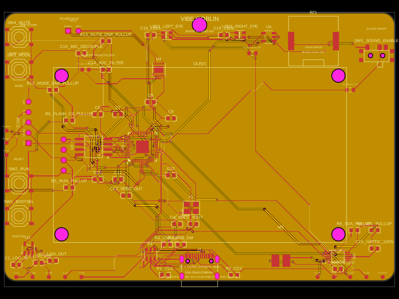 More from this authorAnasSarkiz/vibe_GoblinThese code snippets define various physical electronic components such as ICs, connectors, sensors, LEDs, and chips, specifying their pin layouts, footprint pads, silkscreen markings, courtyard outlines, and 3D CAD models for placement on PCB boards.
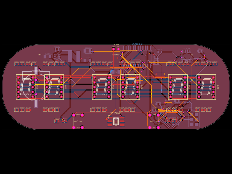 Similar packagegokul/six-digit-logic-clockThis code defines the physical layout and schematic connections for a multi-layer PCB featuring components like RTC modules (DS3231MZ), microcontroller (ATMEGA328P), LED display driver (MAX7219), and various passive and discrete components, with detailed footprints, pinouts, and placement for a clock and control interface.
 Discover something newhrithik18k/smart-switch-pcbThe AO3400A component models a SOT-23 N-channel MOSFET with labeled pins for Gate, Source, and Drain, including 3D CAD models and schematic symbols for electronic circuit design.